This post is part of a longer-running series about giving users a tangible reason to trust their hardware through my IRIS (Infra-Red, in-situ) technique. IRIS allows us to see the insides of certain types of chips, even after they are soldered to a circuit board. This is possible because under infrared light, silicon is practically transparent:
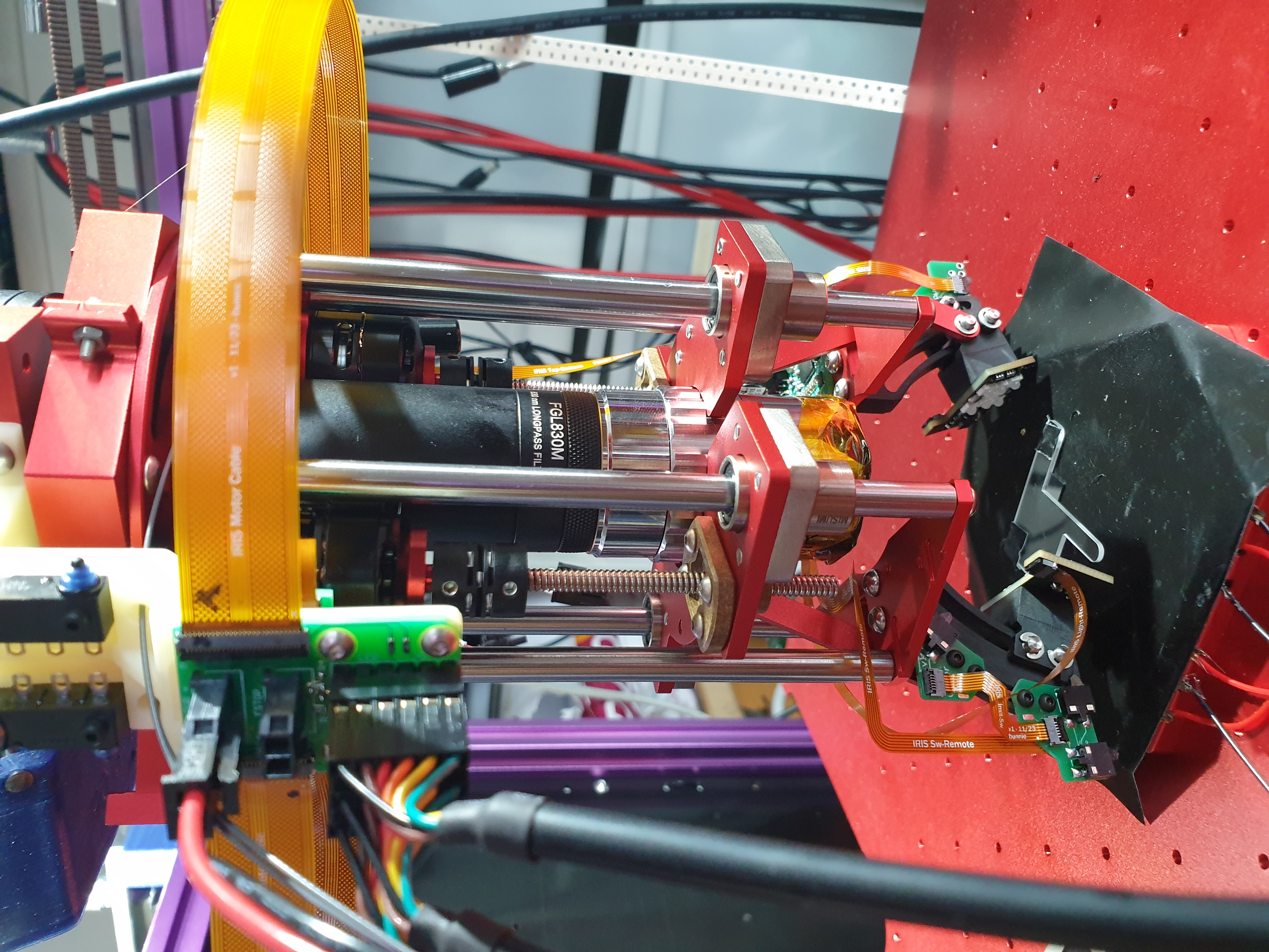
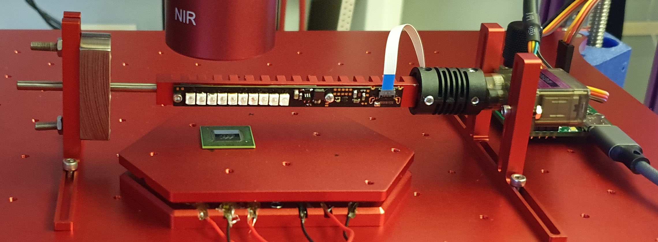
And this is what the current generation of IRIS machinery looks like:
Previously, I introduced the context of IRIS, and touched on my general methods for learning and exploring. This post will cover how I arrived at the final design for the light source featured in the above machine. It is structured as a case study on the general methods for learning that I covered in my previous post, so if you see foofy statements about “knowing it” or “being ignorant of it”, that’s where it comes from. Thus, this post will be a bit longer and more circuitous than usual; however, future posts will be more direct and to the point.
Readers interested in the TL;DR can scroll past most of this post and just look at the pretty pictures and video loops near the bottom.
As outlined in my methods post, the first step is to make an assessment of what you know and don’t know about a topic. One of the more effective rhetorical methods I use is to first try really hard to find someone else who has done it, and copy their work.
Try Really Hard to Copy Someone Else
As Tom Knight, my PhD advisor, used to quip, “did you know you could save a whole afternoon in the library by spending two weeks in the lab?” If there’s already something out there that’s pretty close to what I’m trying to do, perhaps my idea is not as interesting as I had thought. Maybe my time is better spent trying something else!
In practice, this means going back to the place where I had the “a-ha!” moment for the idea, and reading everything I can find about it. The original idea behind IRIS came from reading papers on key extraction that used the Hamamatsu Phemos series of failure analysis systems. These sophisticated systems use scanning lasers to non-destructively generate high-resolution images of chips with a variety of techniques. It’s an extremely capable system, but only available to labs with multi-million dollar budgets.
Above: except from a Hamamatsu brochure. Originally retrieved from this link, but hosted locally because the site’s link structure is not stable over time.
So, I tried to learn as much as I could about how it was implemented, and how I might be able to make a “shallow copy” of it. I did a bunch of dumpster-diving and acquired some old galvanometers, lasers, and a scrapped confocal microscope system to see what I could learn from reverse engineering it (reverse engineering is especially effective for learning about any system involving electromechanics).

However, in the process of reading articles about laser scanning optics, I stumbled upon Fritzchens Fritz’s Flickr feed (you can browse a slideshow of his feed, above), where he uses a CMOS imager (i.e. a Sony mirrorless camera) to do bulk imaging of silicon from the backside, with an IR lamp as a light source. This is a perfect example of the “I am ignorant of it” stage of learning: I had negative emotions when I first saw it, because I had previously invested so much effort in laser scanning. How could I have missed something so obvious? Have I really been wasting my time? Surely, there must be a reason why it’s not widely adopted already… I recognized these feelings as my “ignorance smell”, so I pushed past the knee-jerk bad feelings I had about my previously misdirected efforts, and tried to learn everything I could about this new technique.
After getting past “I am ignorant of it” and “I am aware of it”, I arrived at the stage of “I know of it”. It turns out Fritz’s technique is a great idea, and much better than anything I had previously thought of. So, I abandoned my laser scanner plan and tried to move to the stage of “tried it out” by copying Fritzchen Fritz’s setup. I dug around on the Internet and found a post where some details about his setup were revealed:
I bought a used Sony camera from Kolari Vision with the IR filter removed to try it out (you can also swap out the filter yourself, but I wanted to be able to continue using my existing camera for visible light photos). The results were spectacular, and I shared my findings in a short arXiv paper.
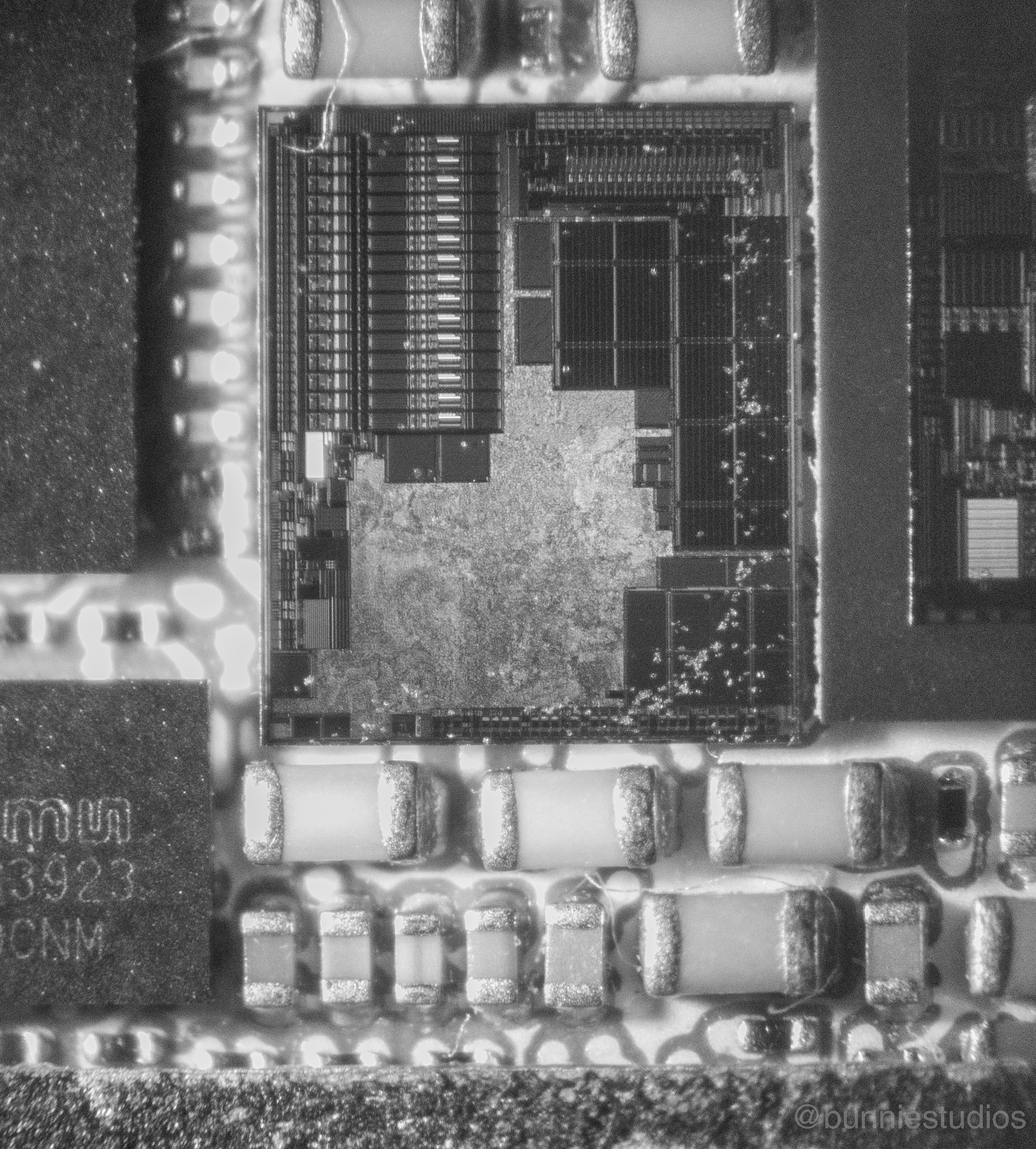
Above is an example of an early image I collected using a Sony camera photographing an iPhone6 motherboard. The chip’s internal circuitry isn’t overlaid with Photoshop — it’s actually how it appears to the camera in infrared lighting.
Extending the Technique
Now that I was past the stage of “I have tried it out”, it was time to move towards “I know it” and beyond. The photographs are a great qualitative tool, but verification requires something more quantitative: in the end, we want a “green/red light” indicator for if a chip is true to its blueprint, or not. This would entail some sort of automated acquisition and analysis of a die image that can put tight bounds on things like the number of bits of RAM or how many logic gates are in chip. Imaging is just one part of several technologies that have to come together to achieve this.
I’m going to need:
- A camera that can image the chip
- A light source that can illuminate the chip
- A CNC robot that can move things around so we can image large chips
- Stitching software to put the images together
- Analysis software to correlate the images against designs
- Scan chain techniques to complement the gate count census
Unfortunately, the sensors in Sony’s Alpha-NEX cameras aren’t available in a format that is easily integrated with automated control software. However, Sony CMOS sensors from the Starvis2 line are available from a variety sources (for example, Touptek) in compact C-mount cases with USB connectors and automation-ready software interfaces. The Starvis2 line targets the surveillance camera market, where IR sensitivity is a key feature for low-light performance. In particular, the IMX678 is an 8-Mpix 16:9 sensor with a response close to 40% of peak at 1000nm (NB: since I started the project, Sony’s IMX676 sensor is now also available (see E3ISPM12000KPC), a 12-Mpix model with a 1:1 aspect ratio that would be a better match for the imaging I’m trying to do; I’m currently upgrading the machine to use this). While there are exotic and more sensitive III-V NIR sensors available, after talking to a few other folks doing chip imaging, I felt pretty comfortable that these silicon CMOS cameras were probably the best sensors I could get for a couple hundred dollars.
With the camera problem fully constrained within my resource limits, I turned my attention to the problems of the light source, and repeatability.
Light Sources Are Hard
The light source turns out to be the hard problem. Here are some of the things I learned the hard way about light sources:
- They need to be intense
- They need to be uniform
- Because of the diffractive nature of imaging chips, the exact position of the light source relative to the sample turns out to be critical. Viewing a chip is like looking at a hologram: the position of your eyes changes the image you see. Thus, in addition to X, Y and Z positioning, I would need azimuth and zenith controls.
- For heavily doped substrates (as found on Intel chips), spectral width is also important, as it seems that backscatter from short wavelength sidebands quickly swamp the desired signal (note: this mechanism is an assumption, I’m not 100% sure I understand the phenomena correctly)
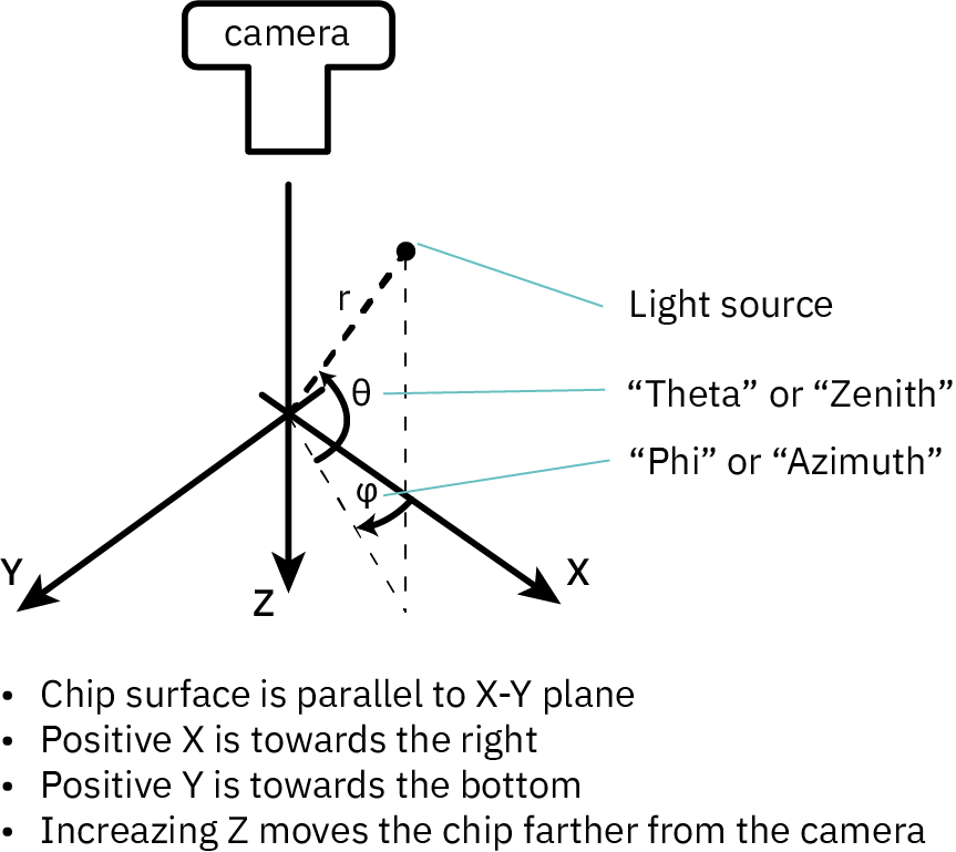
Above is the coordinate system used by IRIS. I will frequently refer to theta/zenith and phi/azimuth to describe the position of the lightsource in the following text.
Of course, when starting out, I didn’t know what I didn’t know. So, to get a better feel for the problem, I purchased an off-the-shelf “gooseneck” LED lamp, and replaced the white LEDs with IR LEDs. Most LED lamps with variable intensity use current-based regulation to control the white LEDs, which means it is probably safe to swap the white LEDs for IR LEDs, so long as the maximum current doesn’t exceed the rating of the IR LEDs. Fortunately, most IR LEDs can handle a higher current relative to similarly packaged white LEDs, since they operate at a lower forward voltage.
With these gooseneck-mounted IR LEDs, I’m able to position a light source in three dimensional space over a chip, and see how it impacts the resulting image.
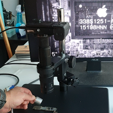
Above: using gooseneck-mounted IR LEDs to sweep light across a chip. Notice how the detail of the circuitry within the chip is affected by small tweaks to the LED’s position.
Sidebar: Iterate Through Low-Effort Prototypes (and not Rapid Prototypes)
With a rough idea of the problem I’m trying to solve, the next step is build some low-effort prototypes and learn why my ideas are flawed.
I purposely call this “low-effort” instead of “rapid” prototypes. “Rapid prototyping” sets the expectation that we should invest in tooling so that we can think of an idea in the morning and have it on the lab bench by the afternoon, under the theory that faster iterations means faster progress.
The problem with rapid prototyping is that it differs significantly from production processes. When you iterate using a tool that doesn’t mimic your production process, what you get is a solution that works in the lab, but is not suitable for production. This conclusion shouldn’t be too surprising – evolutionary processes respond to all selective pressures in the environment, not just the abstract goals of a project. For example, parts optimized for 3D printing consider factors like scaffolding, but have no concern for undercuts and cavities that are impossible to produce with CNC processes. Meanwhile CNC parts will gravitate toward base dimensions that match bar stock, while minimizing the number of reference changes necessary during processing.
So, I try to prototype using production processes – but with low-effort. “Low-effort” means reducing the designer’s total cognitive load, even if it comes at the cost of a longer processing time. Low effort prototyping may require more patience, but also requires less attention. It turns out that prototyping-in-production is feasible, and is actually the standard practice in vibrant hardware ecosystems like Shenzhen. The main trade-off is that instead of having an idea that morning and a prototype on your desk by the afternoon, it might take a few days. And yes – of course there ways to shave those few days down (already anticipating the comments informing me of this cool trick to speed things up) – but the whole point is to not be distracted by the obsession of shortening cycle times, and spend more attention on the design. Increasing the time between generations by an order of magnitude might seem fatally slow for a convergent process, but the direction of convergence matters as much as the speed of convergence.
More importantly, if I were driving a PCB printer, CNC, or pick-and-place machine by myself, I’d be spending all morning getting that prototype on my desk. By ordering my prototypes from third party service providers, I can spend my time on something else. It also forces me to generate better documentation at each iteration, making it easier to retrace my footsteps when I mess up. Generally, I shoot for an iteration to take 2-4 weeks – an eternity, I suppose, by Silicon Valley metrics – but the two-week mark is nice because I can achieve it with almost no cognitive burden, and no expedite fees.
I then spend at least several days to weeks characterizing the results of each iteration. It usually takes about 3-4 iterations for me to converge on a workable solution – about a few months in total. I know, people are often shocked when I admit to them that I think it will take me some years to finish this project.
A manager charged with optimizing innovation would point out that if I could cut the weeks out where I’m waiting to get the prototype back, I could improve the time constant on an exponential and therefore I’d be so much more productive: the compounding gains are so compelling that we should drop everything and invest heavily in rapid prototyping.
However, this calculus misses the point that I should be spending a good chunk of time evaluating and improving each iteration. If I’m able to think of the next improvement within a few minutes of receiving the prototype, then I wasn’t imaginative enough in designing that iteration.
That’s the other failure of rapid prototyping: when there’s near zero cost to iterate, it doesn’t pay to put anything more than near zero effort into coming up with the next iteration. Rapid-prototyping iterations are faster, but in much smaller steps. In contrast, with low-effort prototyping, I feel less pressure to rush. My deliberative process is no longer the limiting factor for progress; I can ponder without stress, and take the time to document. This means I can make more progress every step, and so I need to take fewer steps.
Alright, back to the main story — how we got to this endpoint:

The First Low-Effort Prototypes
I could think of two ways to create a source of light that had a controllable azimuth and zenith. One is to mount it to a mechanism that physically moves the light around. The other is to create a digital array of lights with lights in every position, and control the light source’s position electronically.
When I started out, I didn’t have a clue on how to build a 2-axis mechanical positioner; it sounded hard and expensive. So, I gravitated toward the all-digital concept of creating a hemispherical dome of LEDs with digitally addressable azimuth and zenith.
The first problem with the digital array approach is the cost of a suitable IR LED. On DigiKey, a single 1050nm LED costs around $12. A matrix of hundreds of these would be prohibitively expensive!
Fortunately, I could draw from prior experience to help with this. Back when I was running supply chain operations for Chibitronics, I had purchased over a million LEDs, so I had a good working relationship with an LED maker. It turns out the bare IR LED die were available off-the-shelf from a supplier in Taiwan, so all my LED vendor had to do was wirebond them into an existing lead frame that they also had in stock. With the help of AQS, my contract manufacturing partner, we had two reels of custom LEDs made, one with 1050nm chips, and another with 1200nm chips. This allowed me to drop the cost of LEDs well over an order of magnitude, for a total cost that was less than the sample cost of a few dozen LEDs from name-brand vendors like Marubeni, Ushio-Epitex, and Marktech.
With the LED cost problem overcome, I started prototyping arrays using paper and copper tape, and a benchtop power supply to control the current (and thus the overall brightness of the arrays).
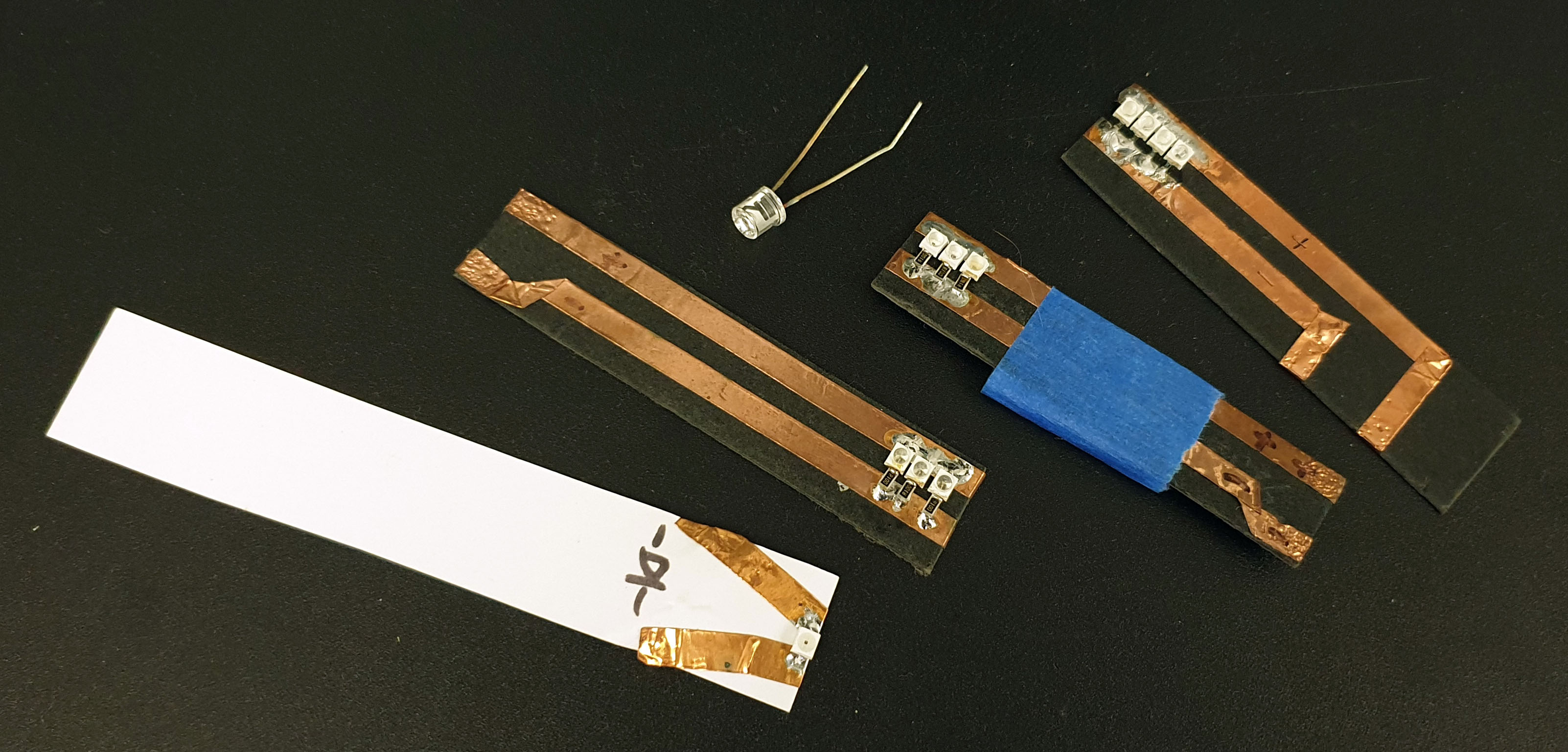
Above: some early prototypes of LEDs mounted on paper using copper tape and a conventional leaded LED for comparison.
Since paper is flexible, I was also able to prototype three dimensional rings of LEDs and other shapes with ease. Playing with LEDs on paper was a quick way to build intuition for how the light interacts with the silicon. For example, I discovered through play that the grain of the polish on the backside of a chip can create parasitic specular reflections that swamp out the desired reflections from circuits inside the die. Thus, a 360-degree ring light without pixel switching would have too many off-target specular reflections, reducing image contrast.
Furthermore, since most of the wires on a chip are parallel to one of the die edges, it seemed like I could probably get away with just a pair of orthogonal pixel-based light sources illuminating at right angles to each other. In order to test this theory, I decided to build a compact LED bar with individually switchable pixels.
Evolving From Paper and Tape to Circuit Boards
As anyone who has played with RGB LED tape knows, individually addressable pixels are really easy to do when you have a driver IC embedded inside the LED package. For those unfamiliar with RGB LED tape, here’s a conceptual diagram of its construction:
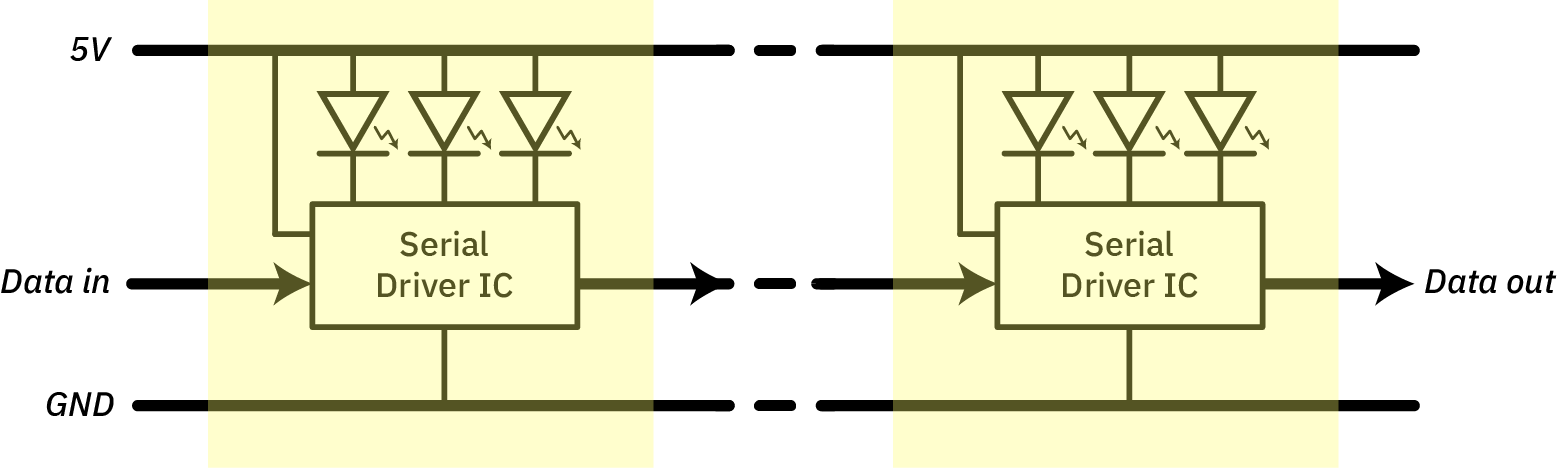
Each RGB triple of LEDs is co-packaged with a controller chip (“serial driver IC”), that can individually control the current to each LED. The control chip translates serial input data to brightness levels. This “unit cell” of control + LEDs can be repeated hundreds of times, limited primarily by the resistance of copper wire, thanks to the series wiring topology.
What I wanted was something like this, but with IR LEDs in the package. Unfortunately, each IR LED can draw up to 100mA – more than an off-the-shelf controller IC can handle – and my custom LEDs are just simple, naked LEDs in 3528 packages. So, I had to come up with some sort of control circuit that allowed me to achieve pixel-level control of the LEDs, at a high brightnesses, without giving up the scalability of a serial topology.
Trade-Offs in Driver Topologies
For lighting applications, it’s important that every LED shines with equal brightness. The intensity of an LED’s light output is correlated with the current flowing through it; so in general if you have a set of LEDs that are from the same manufacturing process and “age” (hours illuminated), they will emit the same flux of light for the same amount of current. This is in contrast to applying the same voltage to every LED; in the scenario of a constant voltage, minute structural variations between the LEDs and local thermal differences can lead to exponential differences in brightness.
This means that, in general, we can’t wire every LED in parallel to a constant voltage; instead, every LED needs a regulator that adjusts the voltage across the LED to achieve the desired fixed current level.
Fortunately, this problem is common enough that there are several inexpensive, single-chip offerings from major chip makers that provide exactly this. A decade ago this would have been expensive and hard, but now one can search for “white LED driver IC” and come up with dozens of options.
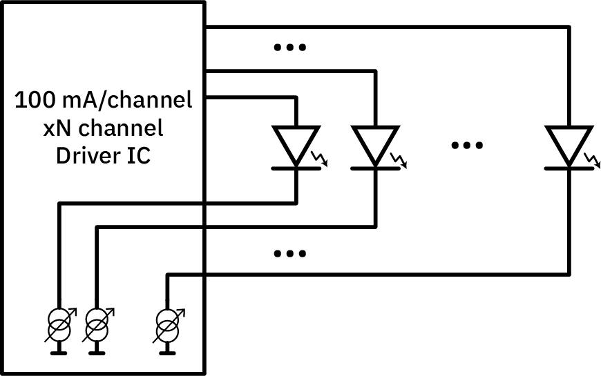
The conceptually simplest way of doing this – giving each LED its own current regulator – does not scale well, because for N LEDs, you need N regulators with 2N wires. In addition to the regulation cost scaling with the number of LEDs, the wire routing becomes quite problematic as the LED bar becomes longer.
Parallel, switchable LED drive concept. N.B.: The two overlapping circles with an arrow through it is the symbol I learned for a variable current source.
Because of this scaling problem, the typical go-to industry technique for driving an array of identical-illumination LEDs is to string them in series, and use a single boost regulator to control the current going through the entire chain; the laws of physics demands that a string of LEDs in series all share the same current. The regulator adjusts the total voltage going into the string of LEDs, and nature “figures out” what the appropriate voltage is for every individual LED to achieve the desired current.
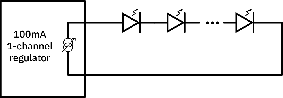
This series arrangement, shown above, allows N LEDs to share a single regulator, and is the typical solution used in most LED lamps.
Of course, with all the LEDs in series, you don’t have a switchable matrix of LEDs – reducing the current through one LED means the current through all the others identically!
The way to switch off individual LEDs in series is to short out the LEDs that should be turned off. So, conceptually, this is the circuit I needed:
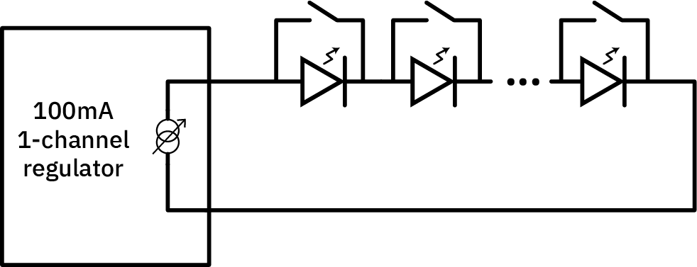
In the above diagram, every LED has an individual switch that can shunt current around the LED. This has some problems in practice; for example, if all the LEDs are off, you have a short to ground, which creates problems for the boost regulator. Furthermore, switching several LEDs on and off simultaneously would require the regulator to step its voltage up and down quickly, which can lead to instability in the current regulation feedback loop.
Below is the actual, practical implementation of this idea:
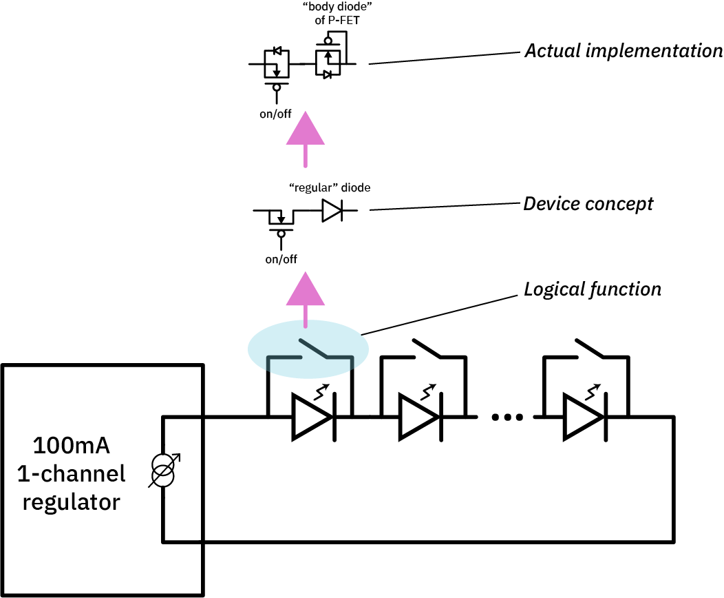
Here, the logical function undergoes two steps of transformation to achieve the final circuit.
First, we implement the shunt switch using a P-channel FET, but also put a “regular” diode in series with the P-FET. The “regular” diode is chosen such that it has a lower forward voltage than the LED, but only just slightly lower. Because diodes have an exponential current flow with voltage, even a slightly lower voltage conventional diode in parallel with with an LED will effectively steal all the current from the LED and turn it off. In this case, instead of emitting light, all the current is turned into waste heat. While this is inefficient, it has the benefit that the current regulator loop transient is minimized as LEDs turn on and off, and also when all the LEDs are off, you don’t have a short to ground.
Finally, we implement the “regular” diode by abusing the P-channel FET. By flipping the P-channel FET around (biasing the drain higher than the source) and connecting the FET in the “off” state, we activate the intrinsic “body diode” of the P-channel FET. This is an “accidental” diode that’s inherent to the structure of all MOSFETs, but in the case of power transistors, device designers optimize for and specify its performance since it is used by circuit designers to do things like absorb the kick-back of an inductive load when it is suddenly switched off.
Using the body diode like this has several benefits. First, the body diode is “bad” in the sense that it has a high forward voltage. However, for this application, we actually want a high forward voltage: our goal is to approach the forward voltage of an LED (about 1.6V), but be slightly less than that. This requirement is the opposite of what most discrete diodes optimize for: most diodes optimize for the lowest possible forward voltage, since they are commonly used as power rectifiers and this voltage represents an efficiency loss. Furthermore, the body diode (at least in a power transistor) is optimized to handle high currents, so, passing 100mA through the body diode is no sweat. We also enjoy the enhanced thermal conductivity of a typical power transistor, which helps us pull the waste heat out. Finally, by doubling-down on a single component, we reduce our BOM line-item count and overall costs. It actually turns out that P-channel power FETs are cheaper per device, and come in far smaller packages, than diodes of similar capability!
With this technique, we’re actually able to fit the entire circuity of the switch PFET, diode dummy load, an NFET for gate control, and a shift-register flip-flop underneath the footprint of a single 3528 LED, allowing us to create a high-density, high-intensity pixel-addressable IR LED strip.
First Version
On the very first version of the strip, I illuminated two LEDs at a time because I thought I would need at least two LEDs to generate sufficient light flux for imaging. The overall width of the LED strip was kept to a minimum so the strip could be placed as close to the chip as possible. Each strip was placed on a single rotating axis driven by a small hobby servo. The position of the light on the strip would approximate the azimuth of the light, and the angle of the axis of the hobby servo would approximate the zenith. Finally, two of these strips were intended to be used at right angles to improve the azimuth range.
As expected, the first version had a lot of problems. The main source of problems was a poor assumption I made about the required light intensity: much less light was needed than I had estimated.
The optics were evolved concurrently with the light source design, and I was learning a lot along the way. I’ll go into the optics and mechanical aspects in other posts, but the short summary is that I had not appreciated the full impact of anti-reflective (AR) coatings (or rather, the lack thereof) in my early tests. AR coatings reduce the amount of light reflected by optics, thus improving the amount of light going in the “right direction”, at the expense of reducing the bandwidth of the optics.
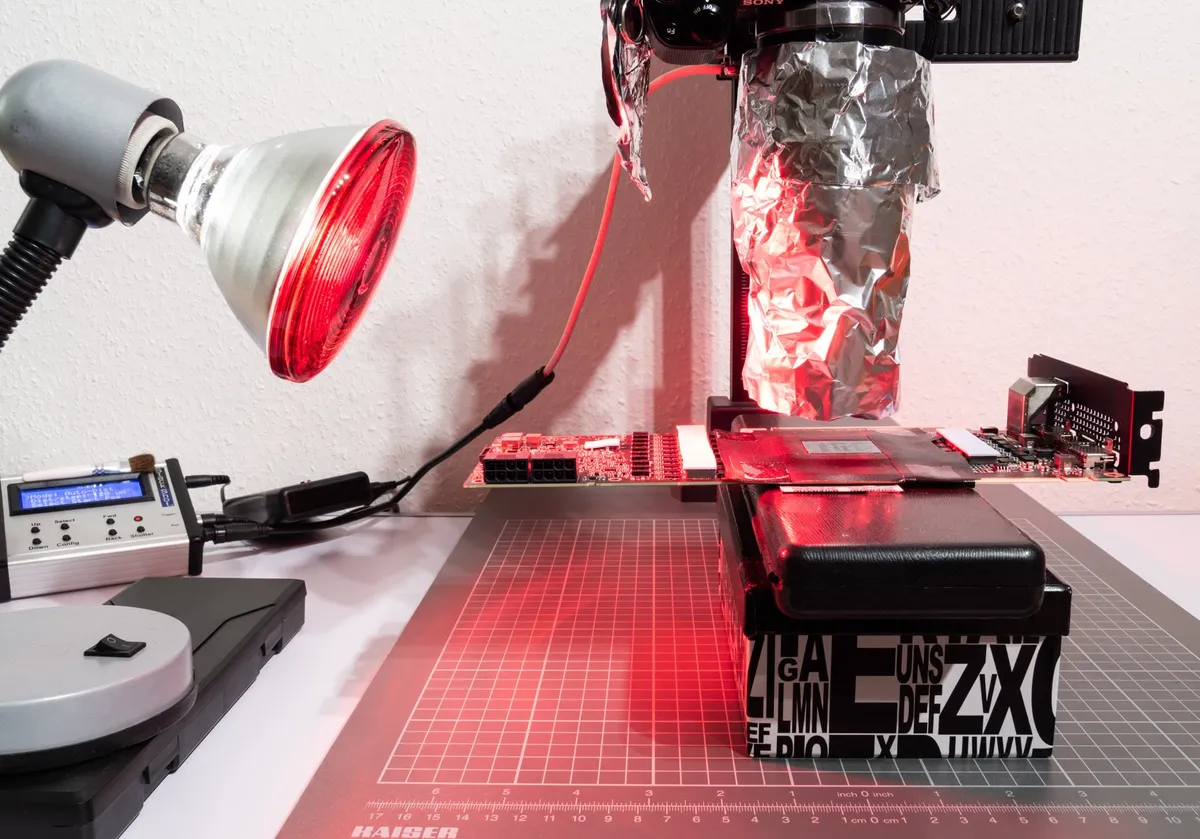
In particular, my very first imaging tests were conducted using a cheap monocular inspection microscope I had sitting around, purchased years ago on a whim in the Shenzhen markets. The microscope is so cheap that none of the optics had anti-reflective coatings. While it performs worse than more expensive models with AR coating in visible light, I did not appreciate that it works much better than other models with AR-coating in the infra-red wavelengths.
The second optical testbench I built used the cheapest compound microscope I could find with a C-mount port, so I could play around with higher zoom levels. The images were much dimmer, which I incorrectly attributed to the higher zoom levels; in fact, most of the loss in performance was due to the visible-light optimized AR coatings used on all of the optics of the microscope.
When I put together the “final” optics path consisting of a custom monocular microscope cobbled together from a Thorlabs TTL200-B tube lens, SM1-series tubes, and a Boli Optics NIR objective, the impact of the AR coatings became readily apparent. The amount of light being put out by the light bar was problematically large; chip circuitry was being swamped by stray light reflections and I had to reduce the brightness down to the lowest levels to capture anything.
It was also readily apparent that ganging together two LEDs was not going to give me fine enough control of azimuth position, so, I quickly turned around a second version of the LED bar.
Second Version
The second version of the bar re-used the existing mechanical assembly, but featured individually switchable LEDs (instead of pairs of LEDs). A major goal of this iteration was to vet if I could achieve sufficient azimuth control from switching individual LEDs. I also placed a bank of 1200nm LEDs next to 1050nm LEDs. Early tests showed that 1200nm could be effective at imaging some of the more difficult-to-penetrate chips, so I wanted to explore that possibility further with this light source.
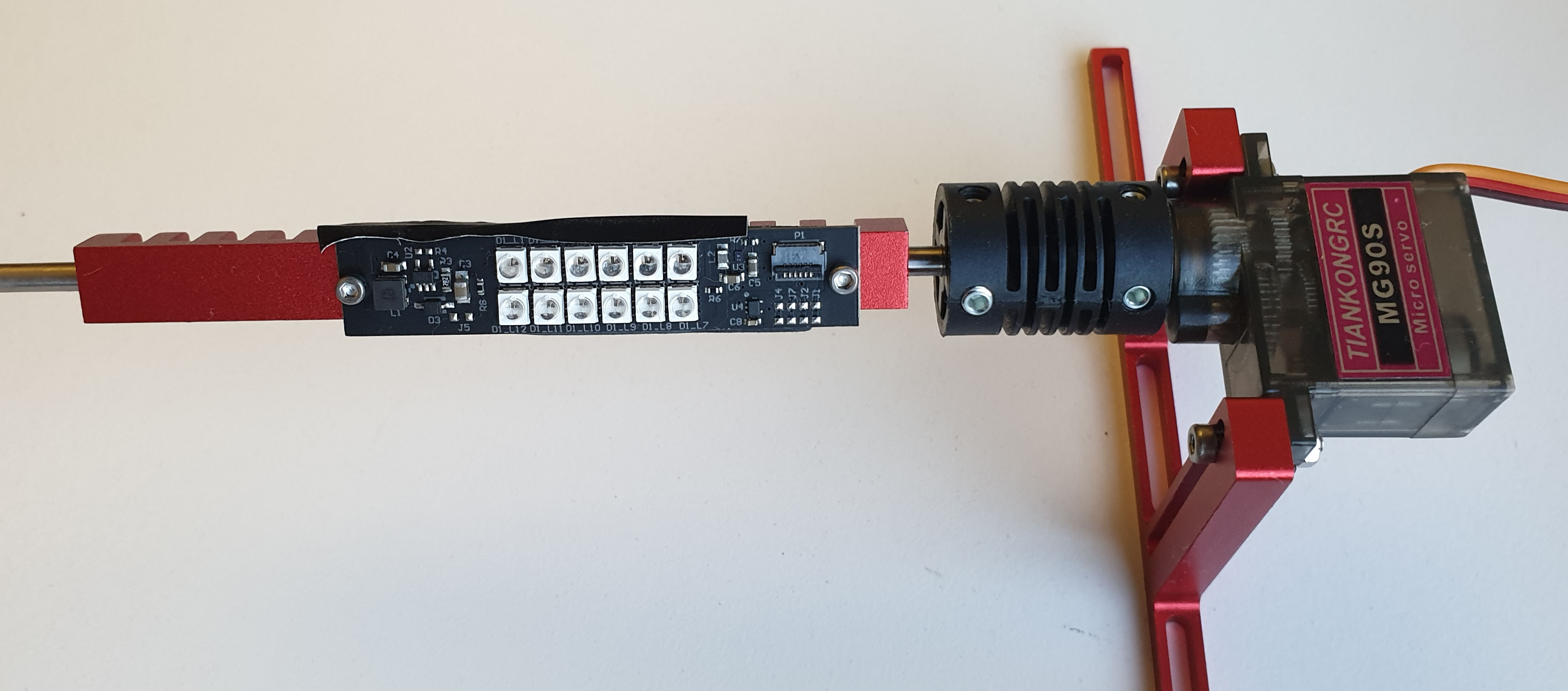
As one can see from the photo above, the second version was just a very slight modification from the first version, re-using most of the existing mounting hardware and circuitry.
While the second version worked well enough to start automated image collection, it became apparent that I was not going to get sufficient angular resolution through an array of LEDs alone. Here are some of the problems with the approach:
- Fixing the LEDs to the stage instead of the moving microscope head means that as the microscope steps across the chip, the light direction and intensity is continuously changing. In other words, it’s very hard to compare one part of a chip to another part of a chip because the lighting angle is fundamentally different, especially on chips larger than a few millimeters on a side.
- While it is trivial to align the LEDs with respect to the wiring on the chip (most wires are parallel to one of the edges of the chip), it’s hard to align the LEDs with respect to the grain of the finish on the back side of the chip.
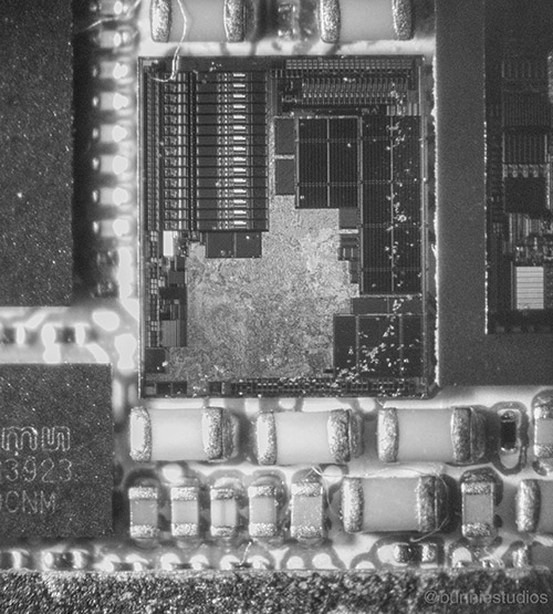
Many chips are not polished, but “back-grinded”. Polished chips are mirror-smooth and image extremely well at all angles; back-grinded chips have a distinct grain to their finish. The grain does not run in any consistent angle with respect to the wires of the chip, and a light source will reflect off of the grain, resulting in bright streaks that hide the features underneath.
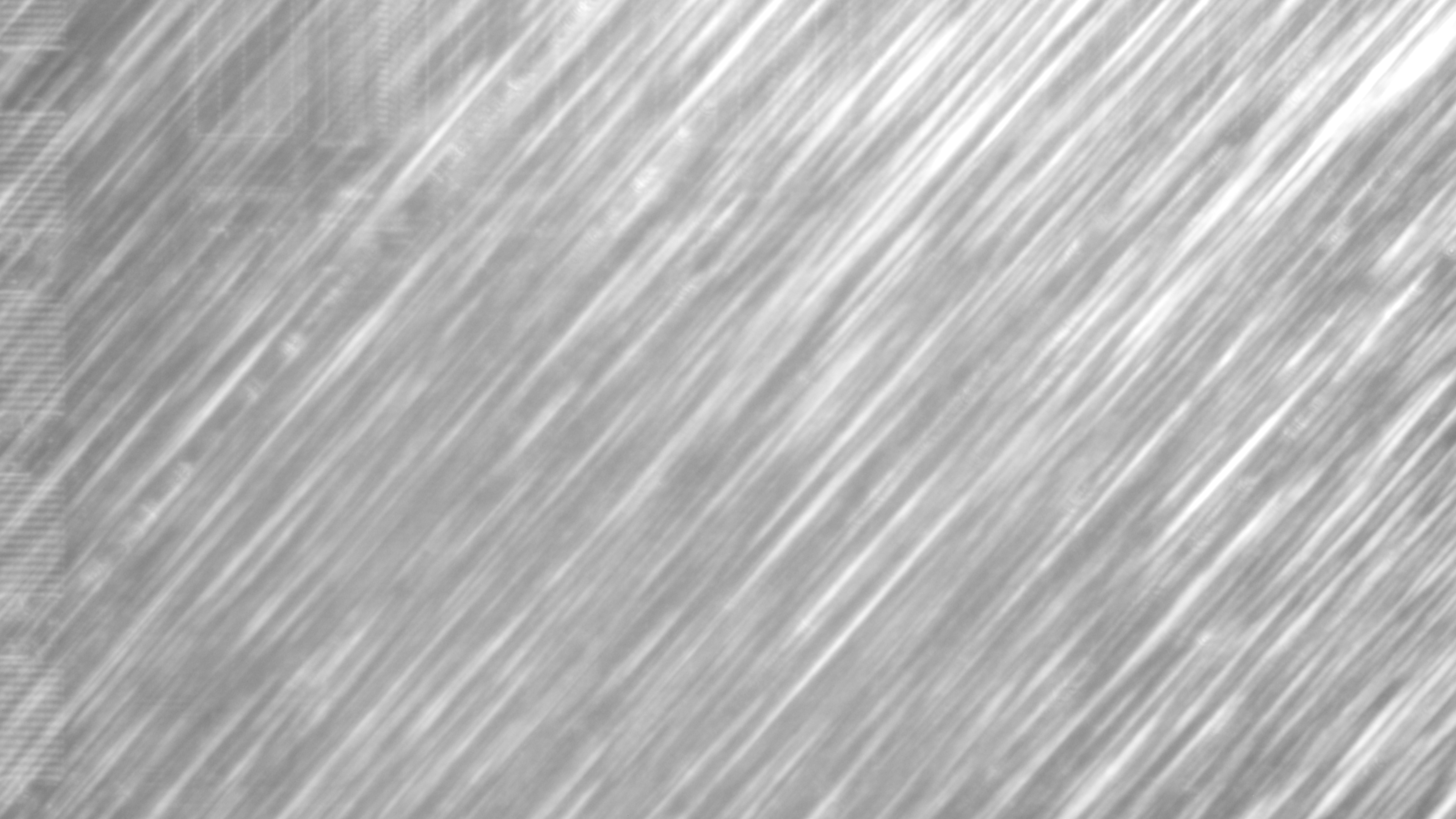
Above is an example of how the grain of a chip’s backside finish can reflect light and drown out the circuit features underneath.
Because of these effects, it ends up being very tricky to align a chip for imaging, involving half an hour of prodding and poking with tweezers until the chip is at just the right angle with respect to the light sources for imaging. Because the alignment is manual and fussy, it is virtually impossible to reproduce.
As a result of these findings, I decided it was time to bite the bullet and build a light source that is continuously variable along azimuth and zenith using mechanically driven axes. A cost-down commercial solution would likely end up using a hybrid of mechanical and electrical light source positioning techniques, but I wanted to characterize the performance of a continuously positionable light source in order to make the call on if and how to discretize the positioning.
Third and Current Version
The third and current version of the light source re-uses the driver circuity developed from the previous two iterations, but only for the purpose of switching between 1050 and 1200nm wavelengths. I had to learn a lot of things to design a mechanically positionable light source – this is an area I had no prior experience in. This post is already quite long, so I’ll save the details of the mechanical design of the light source for a future post, and instead describe the light source qualitatively.
As you can see from the above video loop, the light source is built coaxially around the optics. It consists of a hub that can freely rotate about the Z axis, a bit over 180 degrees in either direction, and a pair of LED panels on rails that follow a guide which keeps the LEDs aimed at the focal point of the microscope regardless of the zenith of the light.
It was totally worth it to build the continuously variable light source mechanism. Here’s a video of a chip where the zenith (or theta) of the light source is varied continuously:
And here’s a more dramatic video of a chip where the azimuth / psi of the light source is varied continuously:
The chip is a GF180 MPW test chip, courtesy of Google, and it has a mirror finish and thus has no “white-out” angles since there is no back-grind texture to interfere with the imaging as the light source rotates about the vertical axis.
And just as a reminder, here’s the coordinate system used by IRIS:
These early tests using continuously variable angular imaging confirm that there’s information to be gathered about the construction of a chip based not just on the intensity of light reflecting off the chip, but also based on how the intensity varies versus the angle of the illumination with respect to the chip. There’s additional “phase” information that can be gleaned from a chip which can help differentiate sub-wavelength features: in plain terms, by rotating the light around the vertical axis, we can gather more information about the type logic cells used in a chip.
In upcoming posts, I’ll talk more about the light positioning mechanism, autofocus and the software pipelines for image capture and stitching. Future posts will be more to-the-point; this is the only post where I give the full evolutionary blow-by-blow of a design aspect, but actually, every aspect of the project took about an equal number of twists and turns before arriving at the current solution.
Taking an even bigger step back, it’s sobering to remember that image capture is just the first step in the overall journey toward evidence-based verification of chips. There are whole arcs related to scan chain methodology and automated image analysis on which I haven’t even scratched the surface; but Rome wasn’t built in a day.
Again, a big thanks goes to NLnet for funding independent, non-academic researchers like me, and their patience in waiting for the results and the write-ups, as well as to my Github Sponsors. This is a big research project that will span many years, and I am grateful that I can focus on doing the work, instead of fundraising and/or metrics such as impact factor.

Would a polarizer film get rid of the bright reflections?
I’ve tried some polarizer films, but I’ve had trouble finding ones that work in the bandwidth I’m imaging in. I suspect it could help in the cases that the grain was at a 45 degree angle from either the horizontal or vertical axis, but as it becomes closer to one of the major axes the grain starts to appear again as you try to illuminate the wires in the chip that are near-parallel to the grain.
There’s also the issue of the intensity loss inherent with polarizing films, but that can be compensated for, to some extent, with a longer exposure time.
Try the wire grid polarizing film from Asahi Khasei.
[…] 详情参考 […]
Did you have to decap the chips?
No. IRIS works on chip-scale packages, i.e., chips that do not require decapsulation, but are already mounted on a circuit board (so the default “interesting side” is facing toward the PCB). Chip scale packages are chips with solder bumps that solder directly on PCBs, and they are fairly popular in mobile phones. It also works on FCBGA, i.e., flip chip BGA packages, which is less common but often found in the realm of high-performance computing.
Awesome. Have you looked yet at Optical Coherence Tomography (OCT) or confocal imaging setups? They could potentially really improve your resolution and contrast in the presence of scattering.