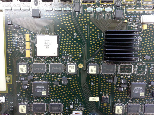
The Ware for February 2015 is shown below.
Eep! I’m late! I blame Chinese New Year.
This one was a tough one to crop: too much makes it too obvious, too little makes it impossible to guess. However, I’m betting that someone out there could probably recognize this ware even if I downsampled all of the part numbers and manufacturer’s logos.
Thanks again to dmo for sharing this ware. I’ll miss visiting your lab!

Looks like an I/O board, 4 parallel I/O channels but only 3 populated, with what looks like 2 PHY’s per channel for a total of 6 populated out of 8 total channels. Based on the buffer memory toward the input side I’d say this is most likely some sort of network switch, with 4 ports handled by a different processor than the other 2… I’m going to go out on a limb and say it’s a blade from an Extreme Networks Alpine 3800 series, maybe a WM-4T1? That has 4 T1 interfaces and 2 FastEthernet interfaces.
Based on the part number format and pixelated logos, the ware was made by HP.
Looks like it’s from an HP/Agilent 16600A logic analyzer.
definitely a timing/state capture card from an early/mid 90s HP logic analyzer. I’d guess the 16500B though :)
Going by the channel count it looks like it is from a 16502A, which is the 102 channel version. We can see that only 3 of the 4 visible channel groups are installed.
From this ebay listing http://www.ebay.ca/itm/HP-16600-66503-Module-for-HP-Agilent-16601A-Logic-Analyzer-/251840131961?pt=LH_DefaultDomain_0&hash=item3aa2d77379 it is apparent that the full version has 3 of the large heatsinked chip in the center for 204 channels.
This is the main acquisition board for the logic analyzer. At top of frame we can see the interface chips for the LA pods. The data flows down to the Acquisition/Trigger chips at mid frame and is stored to the MT58LC32K32B3-10 SRAMs, which are mirrored on the backside to meet the speed and depth requirements (125MHz/64K). The RAM is right at the edge of it’s rated speed of 66MHz.
At the bottom of frame is some more SRAM from NEC. I’m uncertain what it is used for.
From the Ebay listing it is apparent that there are only 2 sets of the NEC ram, but 3 sets of the Micron. Everything is tied together with a bunch of Altera EPM7000 series CPLDs and also a FLEX FPGA.
If you look at the backside picture on the Ebay listing you can see the massive multidrop parallel trigger bus between the Aquisition/Trigger chips.
That was fast!
Correction, the model number it is out of should be 16602A, not 16502A. Looks like these were non-modular logic analyzers built out the same basic architecture as the modular 16700 series. Best guess on the chipset is that it is most similar to the 16711A.
Impressive knowledge!
Controlcard for multiprogrammer.
This is probably an early prototype of the Novena Computing Platform 2015. Dual fpga, new Lowrisc 64-bit with RISC-V instruction set architecture, 160 Gs/s ADC… Bunnie, you are beating yourself!
Every version looks more like a data acquisition board.
Hey Bunnie, who said you can’t visit the lab anymore?! You are always welcome! In fact, you should come and visit the new lab!!
Trick question, it’s a satellite photo of a year 2200 suburb.
(But seriously, the pixelisation doesn’t hide the HP logo nearly well enough.)
What is the purpose of the gold squares littering the outer layers? The silkscreen may be a bit opaque but I can’t seem to see any vias connecting them to anything.
On a related subject, why all those traces have such a weird direction/shape?
I was wonderin about them too, no vias, just blocks – they might be there to stop people xraying the inner traces (but then why not just put in a ground plane?)
The squares are used to equalize the copper density across the board and especially between layers. Uneven density between layers on opposing sides of the board can cause warping during the manufacturing process. Or so I’ve been told by board designers I know.
Something similar is done in chipmaking, but there it is so that the chemical-mechanical polishing step works evenly. So there it is called CMP fill.
Typing in the number on the big white chip (1FE7-0006) shows it might be a RISC microcontroller chip, the Renesas Technology SH7780.
The year on the datasheet for that is 2008.
The Altera chips are “MAX 7000”, with a 2005 datasheet.
I don’t know what the randomly spread pads are about.
Judging by the symmetrical nature of the board, I’d guess there’s actually 2 processors.
If you look at the left, there’s a hole for hanging the board, or screwing it down.
Going through teardowns of set-top boxes shows that it probably isn’t one of them,
and the amount of computing power is inconsistent anyway.
However, the hole to the left looks like, say, a drive bay.
So it might have a DVD drive/ HDD.
ok im going to guess off the wall here..
just to put something a little different into the mix :)
Im guessing a 90`s HP ECG / EEG / EKG receiver processor..