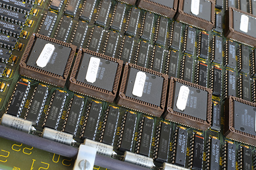
The Ware for September 2020 is shown below.
This is a beautifully photographed ware by David Gingold. When I saw it, I couldn’t let the image go — just had to make it a Name that Ware. Once the solution has been guessed, I’ll add another broader contextual image.
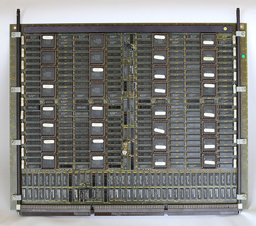
The ware’s been named, so here’s the broader contextual image; I’ll handle the formalities at the end of this month!


Line card from a DMS 100 telephone switch?
It does look like some kind of north American telecom type device. The numbers on the side seem to go to 24 which sounds like timeslots in a T1 line. Could be a line card or a transcoder–PCM to u-law. Given that there’s no external memory and the timeframe of the parts, it’s nothing more complex like ADPCM or GSM. GSM transcoder cards needed a DSP per timeslot and external memory. Even ADPCM would take more than you could fit into a chip that size in the 1984 time frame.
I’d have to stick with the PCM to u-law transcoder for a T1 line guess. Maybe that helps someone else get closer to the answer.
There’s memory. Those INMOS 1420s are 4kx4 SRAMs.
A transputer?
I’d guessed a Connection Machine, for similar reasons.
Hmm: https://www.flickr.com/photos/brewbooks/3320092635/
Oh, NTW July 2016 :-)
> I’d guessed a Connection Machine
That’s the ticket! Here’s A CM-1 chip photo showing the same package and sequential number stickering:
http://www.digibarn.com/collections/parts/connection-machine-chip/index.html
CM-1 had 16 processors per chip with 4Kx1 memory available to each, which matches the board memory array.
-Brian
I was thinking something telephonic. Switch matrix card from a Mitel SX2000?
Observations:
The Inmos parts are fast (for the era) 4kx4 static RAMs, in groups of 8 making 4K x 32.
A bank of memory along the north & south side of each group of four of the mystery 68 pin PLCCs suggests a datapath with one byte per mystery chip.
TTL glue is mostly buffers/registers, the AM2966’s are specialty drivers intended for memory arrays, some ‘138s sprinkled in for decoding.
The marking labels on each mystery PLCC suggest they are programmed in some fashion.
The 84/85 date codes rule out those being modern FPGAs, perhaps a PLD of some sort.
Guesses:
First guess would be a fast static memory or cache board, with the mystery chips implementing ECC.
Next guess would be some sort of datapath processing implemented in the mystery chips that needs two banks of fast local SRAM, not sure what type (don’t know of any ’84 vintage PLDs that could fit an FFT; doesn’t seem like a video board to me)
-Brian
AMD fab used this exact plcc68 plastic molding in eighties/nineties, look up IN80535B, MACH120, or just google image “amd plcc68”.
This could be AMD/Lattice MACH 1 except the dates dont match. MMI merged with AMD in 1987, maybe early custom MMI design? PCB sure looks like transputer, and the dates align, but no gold tops. Then there is the layout suggesting a ton of parallel data being processed and passed, akin to Quantel Paintbox Video effects board.
This looks like something geekdot .com would have a whole writeup on.
A whole range of Inmos transputers, and particularly the Quintek T9/9T bears a strong familial resemblance, but I’ve not found an exact match.
There are 16 of the mystey 68 pin chip on there if that helps anyone figure out what it is. You can tell this because they have an increasing number on each chip and the back row chips are +8 the value of the front row chips which means that there are 8 chips in a rank. We see two ranks, so 16 total chips–unless there is a third rank out of the frame. (I think there is).
IIRC Transputers had a completely different (ceramic) case.
It has several years I used them….