The Ware for April 2021 is shown below.


Both boards are from the same machine. I really admire the construction quality of these boards! Thanks again to Don Straney for contributing these fascinating wares.
This entry was posted on Friday, April 30th, 2021 at 7:00 pm and is filed under name that ware. You can follow any responses to this entry through the RSS 2.0 feed.
Both comments and pings are currently closed.
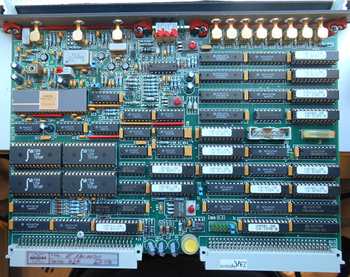
The main board looks like a VXI card for data acquisition, early 90s?
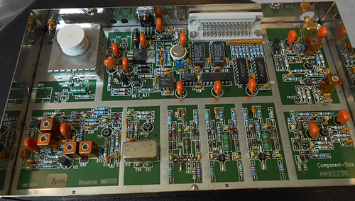
The other board could be generating the high-speed clock signal for the flash ADC.
Is it VXE or VME? I don’t remember them that well.
The bottom board loole like the signal starts at the upper left in that big metal can. Flows down through what looks like a mixer with some filters. Then it flows right through a chain of amplifiers. Finally it goes up the right side and out that RF connection. The upper middle of the board with the DB25 connector has 8 lines of high voltage to TTL voltage conversion with some nearby +/-12V regulators, so I’m guessing something like RS232 or maybe some parallel interface. Looks like there’s got to be at least 8 channels for data there. There’s 9 resistors and a resistor pack of the same size there, so I’d guess 9 channels. Could be 9 inputs (with those resistors serving as a voltage divider) and 8 outputs at +/-12V through the Philips chips. Might be a bidirectional buss as well as those Philips chips have an OE signal. Since I don’t see anything with any brains on it, I’m going to say not RS232, but just some control signals. Maybe to adjust gains or change the frequency of what’s in that can. Hard to tell without seeing the other side of the board.
The digital board is really pretty, too. It’s got a 125MHz 8 bit ADC with an 80MHz ECL can XTAL near it, so let’s assume it’s running at 80MHz. It feeds four (presumeable cascaded) 4Kx9 asyncFIFO chips through a few ECL to TTL converters. There’s a little more ECL logic nearby. Some selectors, some flipflops, etc.
I’m going to assume that every chip with a label on it is a PAL of some sort. There are enough of them to run a few state machines to interface with the bus and manage the data flow. There aren’t enough of them to make up much of a processing system, so I’m guessing there’s no ‘brains’ on this board.
This board looks European. I can’t put my finger on it, but the RF connectors are a type popular there and the choice of component suppliers doesn’t show any kind of regional loyalty. The RF transistors look like European part numbers, too.
I can tell what these boards do, but I’m having a hard time figuring out who designed them.
The spelling “Comonent-Side” also makes it of non native English speaker origin.
Where are you seeing that? On the lower board it’s “Component-Side”. I don’t see anything on the upper board.
It’s the hyphen in component side. In German, it’s usually Bestückungsseite or Lötseite, all in one word. Some Germans hesitate to accept that English works well with separate words and keep the hyphen. Also, the reference designators look German to me: ST for Stecker (connector), T for Transistor (usually labeled Q in English-speaking countries). Many transistors are of European naming heritage (a.k.a. pro-electron, i.e. BF…, BD…) instead of JIS (2S…) or JEDEC (2N…).
Pretty sure that’s the Bruker logo blurred out on the first card’s connector.
Therefore, this must be some kind of high-end data acquisition hardware. (You’re all quite welcome for that startling bit of insight.)
Was going to say the type and layout of the RF connectors on the first board remind me of something I’ve seen before on some MRI or NMR equipment, and it seems like Bruker is a major manufacturer of those things.
I recognize them (or slightly larger variants) from E1 data lines used in Europe from my days designing cell phone base stations. I never looked into what kind of connector it was as I live in NA and they’re nowhere around here.
At this point, it’s pretty clear this is a data capture board from an MRI/NMR system–thanks to Josh M. I saw the logo and tried to find similar ones, but my google failed.
To address J. Peterson’s comments (below?) I would say that using through hole at this point in time means that this was late production for an earlier design. Industries that require approvals tend to not change designs unless they have to. So they tend to be pretty conservative in their component selection–they stick to parts with a long production life even if that costs them in other ways. I would bet you could still source parts to make this board today without much problem. The critical Datel and IDC chips are still available in those packages. The rest is pretty jelly-bean stuff, so I’m sure someone still makes it.
Props to Bruker for their clean design.
Seems you found the make. The exact model for the make is still to be found, but there’s currently an auction for a “Bruker Oxford Spectrospin RCU1/1 AQX ECL06 RCU VME module” that looks much like a slightly more modern version of the ware to be named. Also, there’s a rack called “Bruker Oxford Spectrospin AQR/P 9 Slot H2093 Mainframe AQR ECL00 ECL01 and PSB5” which looks like it might take modules just like the one here?
That looks like one of the CPU modules that does the processing for this series of boards. The two wares posted look like an RF front end (amplifier, mixer, filter, etc.) while the other board is a digitizer and maybe some kind of control/sequencer. It’s got no brains on it more complex than a state machine–from the # of PAL/GAL chips.
True. However, those modules have a similar size and connector layout. When searching for the terms
bruker avance aqs module
one can find racks for NMR spectrometers, and these racks seem to take similar modules. I fail to find an exact match, and I guess this is where I have to stop my efforts – but I guess the boards must be from an early version of Bruker’s Avance series, or maybe a product that was later replaced by the Avance family.
No guess to the origin, but the chip date codes are all reading late ’90s (97 etc.).
What’s really strange is most manufactured items had switched to surface mount components by them (TSOP, QFN, etc), so it’s strange to see everything mounted through-hole 1980s style.
I work in a facility that still relies on a great deal of VME hardware like this that has been running 24/7 for 25+ years. This stuff is over-engineered and built like a tank. It keeps running when the HVAC fails and the ambient temperature hits 95F. Awesome stuff.
I don’t have any startling insights, but I do rather like the way the transistors are mounted in holes in the PCB. That’s a new one on me.
This was/is common for RF transistors. They come in packages that look like they would be surface mount, but the leads aren’t bent down in the classic ‘gull wing’ shape. Instead, they come straight out and the part is mounted in a hole in the PCB so that the leads are on the plane of the copper.
The reason for it is to control impedance of the leads–bends are bad. Some of them aren’t transistors, but more complex amplifier devices. I’m guessing they’re from Mini Circuits. They make a lot of components like that and they also make the metal cased part labled MCL PAS-1. So the designers were aware of MCL, so it’s not unreasonable to think they would use other parts of theirs in the design.
Did you see that building shake
Okay, month’s over, time to speculate. The best I can do is that they’re from the analysis/control system of a:
1.5 Tesla whole body Symphony/Sonata imager (Siemens Medical Systems, Iselin NJ)
or
1.5 Tesla magnet (General Electric Corp, Waukesha WI)
Which probably used Bruker Omega CSI consoles.