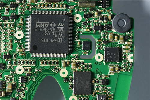
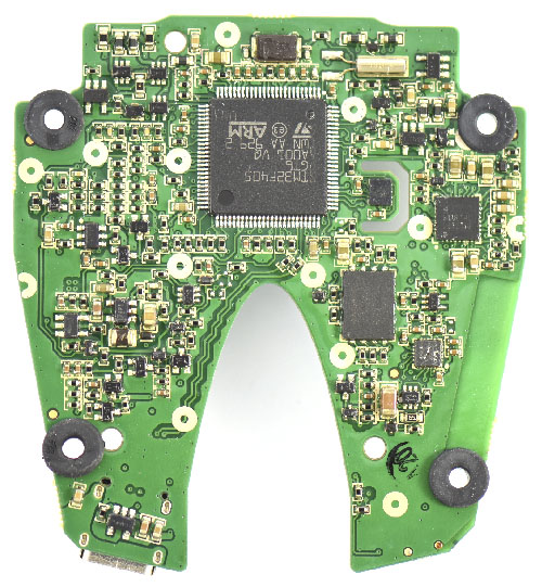
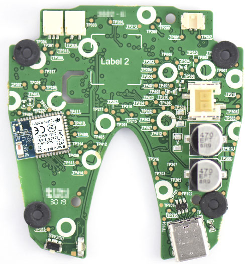
The Ware for March 2023 is shown below:
Thank again to spida for submitting this ware. I was certainly stumped when I first saw it! Again, some very big “clues” are not shown, which I will add to the post later if it turns out to be too difficult to guess.
Hint #1 Update
April 9, 2023: Here’s an additional image, courtesy of spida, that enhances the contrast on some key parts.

I’ll also drop a meta-hint. As is the case for most modern, highly integrated MCU-based wares, any context photo revealing what plugs into the connectors basically gives away the entire function of the ware. If the enhanced image of the circuit board does not converge guesses toward a correct functional class, I’ll add a context photo in roughly one week that should do the trick.
This part of the reason why I personally like looking at vintage wares and test equipment…you can learn a lot just by looking at the circuit board!
Hint #2 Update
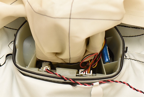
April 16, 2023: Here’s a “context” image hint. This is a picture of the circuit board, installed in its case with all of its peripheral devices plugged in. My assumption is this image should rapidly lead to the ware being guessed, but…this one has been surprisingly difficult so far!


Seems like a detector for markings or the like on the edge of something rotating in the cut-out. My guess would be a controller for some kind of exercise bike.
I’ll say right off that whomever designed this PCB has a lot of experience. This board is impressive. The RF (BT+NRF) module with ground void for the antenna, the diff pair routing, the variable width power runs… This person is on their game.
Interesting choice of devices and I/O on here. We have a pretty capable ARM uC in the middle. There’s the BT+NRF module by Laird Connectivity Inc. There’s a USB-C jack. There’s some beefy capacitors. There’s *vibration mounts*! There’s a routed isolation channel around the high speed XTAL/OSC module for the uC. There’s a button on the prong opposite the USB-C connector next to an LED or some kind of opto sensor facking into the ‘channel’ cut into the board. There’s what can only be an I2C EEPROM of reasonably large capacity next to the uC which is interesting as the micro has enough FLASH to store quite a bit of data. So, they either do a lot of wiring and needed the better endurance of the EEPROM, or they thought there was a price/area tradeoff that made it a better idea then getting a micro with more FLASH.
There’s several connectors. Likely one is for the NRF antenna. The large one by the caps is for the battery I’d guess. Nothing is labeled, so I’m guessing this was in an enclosure that was never meant to be opened–which might explain the apparent adhesive residue on a lot of the chips.
As for its age, the USB-C and RF module make it very modern–last few years at most. The vibration mounts mean it was at lest a portable device if not a mobile one. It was self powered and needed to record a good deal of data and likely relay that to another system. I can’t put my finger on it, but it ‘smells’ medical to me.
I don’t have a ton of time to play this month, so I’m going to wish everyone else luck and I hope I’m not too wrong and my errors throw people off. If so, sorry!
Looks like something to measure light in the cutout. No display, but RF connectivity. has usb-c, a single button. The cutout would nicely fit the assembly of an rc helicopter (and the anti vibration mounts/beefy µC would fit too), or a mouse wheel, but the remaining connectors don’t really fit those use cases, since that would require multiple servo outputs for rc helicopter, or optical sensor for a mouse.
Could it be some kind of barcode reader?
BT, vibration mounts, aerodynamic shape…
Adding to what has already been said/identified:
The connector next to TP601 seems to be power related. It looks like there are ferrtite beads and power-switches (the two sc70-6 packages) next to it on the top side.
I am not sure what all the resistors on the left side of the CPU are for. They look like voltage dividers, but there are just to much of them to just be feedback-dividers for the various voltage regulators.
The CPU has a 32kHz and a ‘fast’ crystal. It might sleep most of the time while keeping a RTC alive.
The USB connector is routed directly to the STM32, so we can’t know which USB-Device-Class is used.
The battery-charger-chip is a ‘LP3921 Battery Charger Management and Regulator Unit with Integrated Boomer™ Audio Amplifier’. It has 7 LDOs, the battery-stuff, and audio-amplifier (BOOMER^^). All of those are wired up and seem to be used. Its has only one channel, so we can rule out any kind of audio-equipment.
I would guess that the audio is used for a some kind of UI, perhaps some speech2text to confirm actions/user-input. So one of the two connectors (next to TP303) is most likely for some kind of speaker.
There is a button and a LED at the bottom of the cutout. I have no clue how they would be used. The LED points inwards, like it would for a photo-interrupter. But there is no receiver, so I think its unlikely to be that.
Perhaps there is some kind of light-guide in the cutout which is illuminated by that LED.
The device seems to be about the size of a hand. TI mentions the following applications for the LP3921:
• CDMA Phone Handsets
• Low Power Wireless Handsets
• Handheld Information Appliances
• Personal Media Players
None of those seem to match. There is no display and no connector for one. The interaction with the user is only a button, audio and bluetooth.
The shock-mounts and glue/whatever residue also don’t match any of those device categories.
I am not sure what the chip on the opposite side of the Bluetooth-Module is and what it might be used for.
So given all of that, my guess is that it is a Babyphone. It has wireless-connection, is somewhat ruggedized and battery operated. There is a temperature sensor, and only minimal UI. The connectors could be for a microphone and speaker.
glad to see i am not totally wrong, many things I’ve been thinking of exactly. What do you think all these resistors are for? Audio channel?
When going with the baby-monitor theory, they might be to set comparator-thresholds. For some kind of voice-activation.
I *think* most of those resistors (?) are a 5×2 matrix. The two rows just to the left of STM32F, just above the “1Ft” NPN, sure seem to be two rows of five chips in parallel, then connected serially. In other words, input, output, and mid-points are shorted. Also, the next two rows to the left (third and fourth left from the STM32F) look like they are voltage dividers, but with one leg actually inmplemented as two resistors in series. So… extreme reduction of unique part types?
Why all the white silk screened circles on both sides?
Is the one led in the slot a light detector to turn it on? Or a light detector to be sure something is closed? With the special care taken to isolate the temperature sensor and all the resistors, it has to be measuring something accurately. Could it be some kind of scale
>Why all the white silk screened circles on both sides?
That’s where the hold-downs press down for the bed-of nails.
Impressive number of test points.
I’m taking a wild gues that it’s a PS5 or XBOX ONE controller PCB?
Nevermind, the USB C isn’t in the right place for that.
Maybe it is a rechargeable bluetooth mouse instead. A lot of those have a USB connector in the front so that they can be used as a wired mouse during charging. Those would also have about the same form factor, and the cut-out would fit a scroll-wheel assembly nicely.
Most of them have the connector straight ahead, but some of the gaming mice have a open split in the middle, and therefore shifts the connector to the side like on this PCB.
Quite the head-scratcher!
My guess is a docking and/or charging station, to store some kind of portable devices between use.
Battery charging could explain the temperature sensor and analogy switching stuff under the big JST connector.
The BLE module seems to also have NFC capabilities, which would chime with a docking station.
The cutout with LED on the side could be for a light pipe for a decorative light-pipe indicating charge state.
It’s either that or a fancy rice cooker. :)
I don’t have anything to add except that it doesn’t make sense for the USB connector to be at the business end of the device if the cutout is a sensor in a portable device, and it’s at a bad angle if that end is a dock.
(Heh. Almost like this is part of a little robot, the wheel fits in the cutout, and the switch is part of a bump sensor? And the location of the USB jack is forced by some form-factor constraint, or bad design esthetic. Except I don’t know what to make of the LED. Where’s the other end of the optical rotation sensor?)
Maybe it is a rechargable bluetooth mouse. The form-factor is about right, and the cut-out would match the scroll-wheel assembly. Many of those have a USB port in the front so they can be used like a wired mouse during charging.
I searched a bit but I could not find any exact matches. Something like https://www.rtings.com/mouse/reviews/vegcoo/c18 , but that mouse had a micro-usb connector instead. Most of them seems to have the cable coming out front-center, instead of out to the side.
Could it be a rugged RFID reader? That would explain the shock mounted PCB board. These products seem tantalizingly close but none seem an exact fit:
https://www.tsl.com/wp-content/uploads/UHF-Reader-Comparison-Infographic.pdf
Bike trip computer/speedometer, maybe?
All those test points make me think this is something designed to be held up as evidence in court cases and is built to be taken apart and checked over and over again… which is why I’m going with breathalyzer.
Cut out is for an airflow meter for the “keep blowing” part…
I’m with Johs, above. I’d say rechargeable wireless mouse.
The cutout at the bottom looks to be designed to accommodate a scroll wheel, and the optical device at the bottom appears to be a side-emitting RGB LED, like a Kingbright APFA3010SEEZGQBDC.
The audio amplifier integrated into the LP39021 threw me for a bit of a loop because I don’t think I’ve ever seen a mouse with an integrated audio device, but I was able to find a Chinese patent for just such a thing. ( https://patents.google.com/patent/CN101071345A/en )
The 32kHz watch crystal at the top of the board would be used by the STM32’s timer circuitry to periodically wake the mouse up from an ultra-low power sleep state to see if the mouse has been moved.
I’ve also found a few mice with vibration motors for haptic feedback. It’s not inconceivable that they could have used the amplifier in a haptic circuit
One piece of evidence against the mouse idea is the lack of an optical sensor nor even a place to connect one. The biggest connector (other than USB-C) has three connections. Is that going to be enough to talk to an optical chip? I’d expect clock+data or clock+data I and O for four and five pins respectively.
Perhaps some fitness device?
More thoughts… I’m only vaguely EE-aware, but this looks like a more-money-than-sense project. Or more precisely, optimization and reliability weren’t actually very important, but following some rules was.
* Shock mounts, but no conformal coating? Resonator hanging out in the breeze? Relatively heavy USB connector cantevered past the rubber mount point, with 1 meg resistor orientated for maximum flex stress? “Tuning fork” (cutout with chip soldered to the tab).
* Tons of test points, to the point of redundancy. (e.g. TP703 & TP706–they expect the ground plane to be bifurcated?) To the point where some of them don’t look well supported and have flex-sensative SMD parts on the opposing face.
* What *is* that cutout for? Certainly not voltage isolation. Doesn’t look like an economical soluction to whatever problem. (Was willmore saying that’s isolation for oscillator?)
* Appears to be a royal pain to get parts approved, as indicated by ridiculous amount of serial- and parallel-connected resistors.
* What’s with that lifted trace? Cheap-ish board quality?
So not avionics or mil-spec. Agree with willmore–smells like high-end home or maybe office medical.
I’m wondering if the board is vertically placed in the end unit, with USB connector towards the bottom. I ran across an air flow monitoring device that had a weird flying-saucer-shaped mouth piece that rotated for use. Something like that, rotating horizontally? Also saw some devices with voice prompts. Maybe that’s what the big ROM is for–multiple languages.
The board looks like it’s conformal coated, but only one one side. You can see a drop of the yellowish coating that ended up on the other side of the board near the TP412 silkscreen. The coating does not cover some of the large IC packages on the component side.
While the construction overall doesn’t seem too rugged, it’s interesting to note that the electrolytic caps used are the automotive-grade Panasonic FT series and are 25V rated. None of the semiconductors seem to be automotive grade parts. The high voltage rating makes sense when considering the TPS6104x boost converter IC (marked PHPI, up to 28V output, 400mA switch current) on the opposite side of the board from them. It’s not too clear what this voltage rail is used for, but it seems likely that it’s related to the large upward-facing connector on the bottom of the board with thick PCB traces coming off of it. One of the traces goes to one of the BC847 NPN transistors (marked 1Ft) on the top side, connected to what seems to be a bunch of 0402 resistors in a 5 parallel – 2 series configuration, possibly for increased power dissipation?
I think the component inside the cutout is more likely a temperature sensor being used to sense ambient air temperature, and the cutout is isolating it from the heat-generating PMIC to the right. I have seen this design technique used before, but only in devices like thermometers and thermostats where accurately measuring ambient temperature is critical. The main oscillator seems to be the large black 5032-package crystal at the top of the board with light gray C0G capacitors on either side.
I wonder if these resistors form an R-2R ladder. Which would be another oddity as the STM32F405 does have a DAC peripheral.
Assuming it’s medical, could this be part of a blood glucose, blood pressure or blood oxygen sensor? Bottom cutout might be fit for a finger, the optical device opposite the Amphenol connector might be for illumination (blood oxygen detection). The chip on the separate tab might be some heated crystal oscillator. The cutout around it would reduce the amount of heat sinking into the PCB.
If only we knew what peripherals are around, connected to the four white jacks? One is probably battery but what about the others?
Perhaps a board out of a pair of noise-cancelling headphones? The rubber points look like they could be a shock-mount inside the earcup housing, and the angle tracks for the USB-C port.
I think it has to be a fingerprint scanner. I can’t find one that looks like an exact fit for the PCB, but this one is close and gives the idea:
https://www.injes.com/rs485-bluetooth-usb-finger-scanner-for-android-iphone-ipad-ios_p47.html
This seems *very* close. Even has the USB cable in the right spot:
https://fingerchip.mainguet.org/periph/AT77C101_ID3_biothentic_atmel.jpg
Maybe a production version of this prototype
Wow, sure looks like it. How did you find it? Interestingly, one of the applications is a medical device–a “smart bottle” that dispenses opiods and such per prescription.
https://www.annuaire-plateforme.ch/fs/documents/Ethimedix%20BTD3%20product.pdf
https://fingerchip.mainguet.org/dispenser/Ethimedix_EPFL_ABo_fig3_SmartBottle.jpg
It has some kind of wireless, but I can’t find any mention of external USB. Attached peripherals are a delivery pump, a locking latch, some kind of anti-tampering “instant neutralization” subsystem, and “two year battery life”, so it’s got to be rechargeable. The jpeg shows a PCB that could concievably have morphed ino something similar to the NtW photos; there’s some kind of connector where the NtW’s USB connection is.
Company looks like it’s currently active, and has a refined product “in pre-clinical stage”.
http://www.ethimedix.com/professionals/
[Bunnie, IMHO this is one of the best Name that Ware puzzles you’ve posted.]
The cutout’s size and shape look about right to accommodate a small centrifuge tube (https://www.thermofisher.com/search/browse/category/us/en/90168054 ). In that case, perhaps the LED would be in a good position to illuminate the a liquid sample contained in the tube, assuming the ware is a handheld device with the cutout meant to be pointed upward.
If one of the peripheral devices turns out to be a spectrometer, or some other kind of optical sensor, perhaps the purpose of this ware is to measure the results for some type of medical, industrial, or agricultural field test kit.
One problem with this guess is, what about the rubber grommets? Why would a handheld spectrometer-ish device need shock mounts? My best guess for that is, maybe the ware’s enclosure is designed to use the PCB as a depth stop for the bottom of the centrifuge tube. Perhaps the shock mounts are meant to help avoid damage if samples are inserted roughly.
I think the small number and pin count of connectors excludes a lot of the previous suggestions for what this thing could be. There’s not enough connections leaving the board for any peripherals to be connected by UART/I2C/SPI, let alone any parallel interfaces.
The two connectors closest to the LP3921 IC seem to be for a battery with temperature sensor (3-pin connector with pins connected to ground, one thin PCB trace, and one thick trace) and a speaker, which seems to be connected through ferrite beads on the opposite side of the PCB.
The other two connectors are less clear, but appear to be some sort of power outputs (big LEDs, small brushed DC motors, solenoids) based on the components they are connected to. The small boost converter with relatively low output current (50mA or less at 24V) combined with relatively large capacitors and fairly beefy traces going into the nearby connector suggest that it’s being used to drive something that either has high inrush current (a motor) or needs intermittent short high-current pulses (an electropermanent magnet?)
The LED near the cutout in the PCB looks like a fairly standard side-mounted two-color indicator LED, like Dialight 5988510207F. Based on that and its position near the switch and USB port I think it’s most likely just an indicator and not too important to the function of the device.
The actuator board for an air bag?
Yup, looks like the board from a Hovding 3 airbag helmet.
I’m surprised at how “consumer-grade” the design and construction quality of this is for a safety device, I would have expected at the very least for more substantial connectors to be used, or for the connectors and electrolytic caps to be covered in silicone for vibration mitigation.
Here’s a link to an ifixit teardown of a Hövding 3 with lots more pictures
https://www.ifixit.com/Teardown/H%C3%B6vding+3+Teardown/156260
Looks like a match to me.
I’m still puzzled about the purpose of the big PCB cutout. A couple pictures in “Step 9” sorta show that area (looking down where the gas generator goes), but with the big white plastic insert still installed. Maybe the PCB cutout is meant to allow for clearance to accommodate mechanical reinforcements around the bottom of the gas generator?