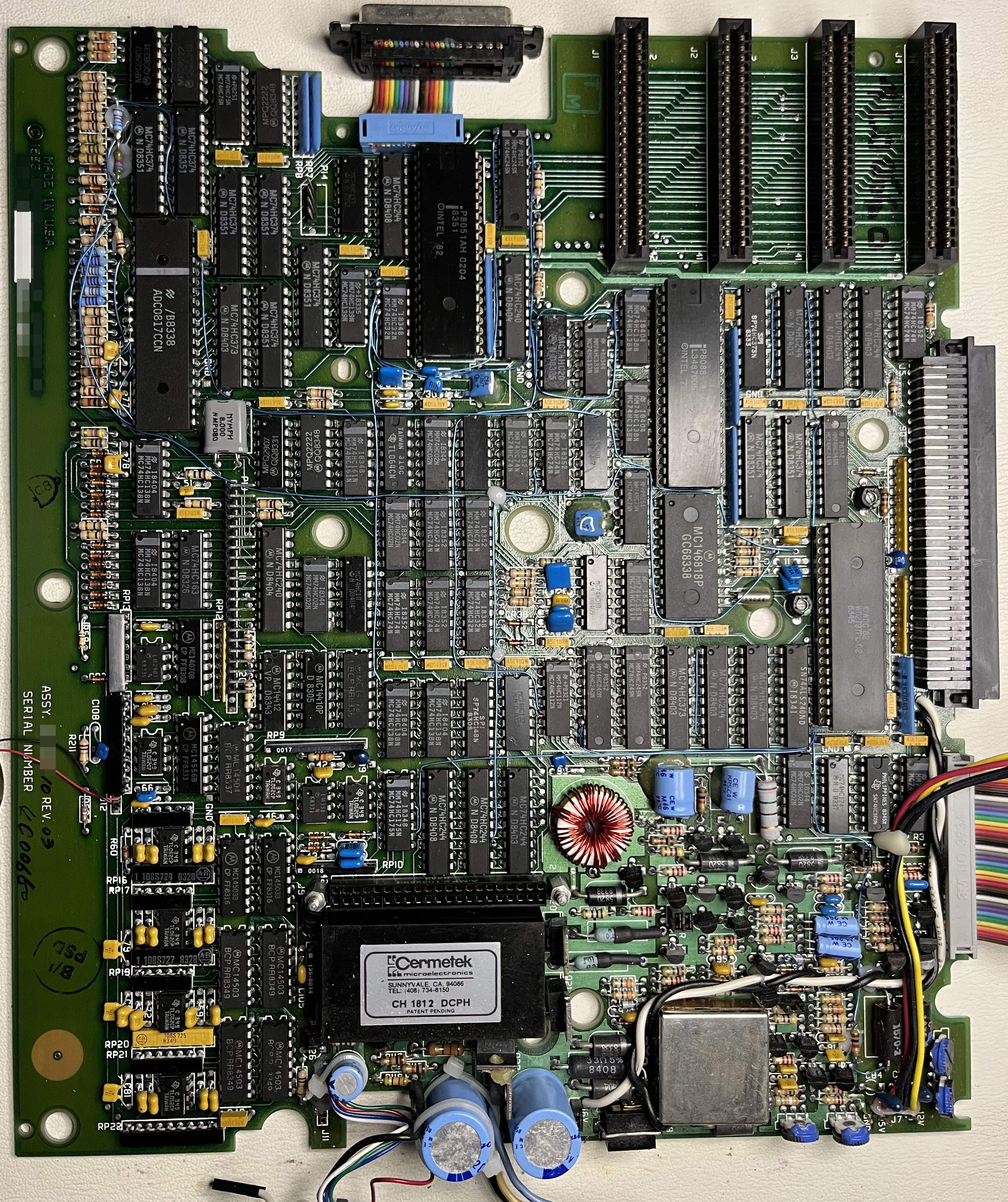
The ware for January 2025 is shown below.
Thanks to brimdavis for contributing this ware! …back in the day when you would get wares that had “blue wires” in them…
One thing I wonder about this ware is…where are the ROMs? Perhaps I’ll find out soon!
Happy year of the snake!
Update Feb 12 2025
Seems to be a stumper. Lots of good analysis, but …
There’s been some mention about seeing the back side of the board; brimdavis was kind enough to provide a nice image of that:
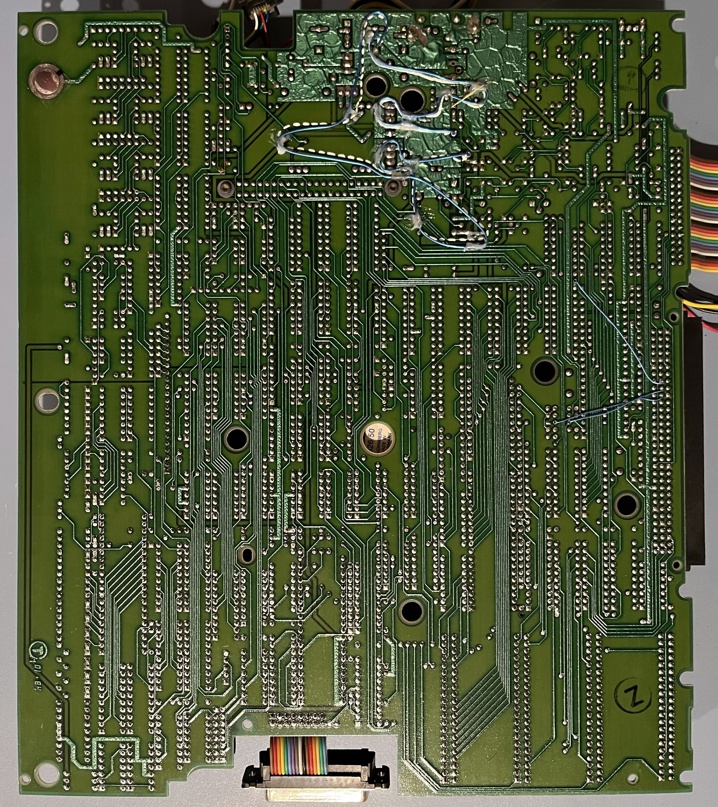
I like how there is a dashed white line for where a blue wire should go.
Also, apparently the “wrinkly” effect is due to a problem “back in the day” where solder wicks under the solder mask during wave soldering? I never got a definitive answer on what causes that, or why modern boards don’t seem to have that issue anymore. In case nobody can guess what this ware is, I’d accept a convincing answer for the wrinkly soldermask mystery as a “tie breaker”.
I’ll drop another hint – brimdavis sent me a contextual photo of the assembly, and the ROM, RAM, and video board plug in through the 42-pin connector just above the telephone line connection unit.
So, to start: we have an 8088 processor with a WD2797 floppy controller up top, an 8051. The original IBM PC used an 8048 for the keyboard, but maybe this clone used an 8051? The ADC0817 at the bottom is an ADC. The expansion slots use 21×2 pins, which isn’t ISA. I don’t want to say this is an IBM PC, because the ADC is quite peculiar.
Searching for “ADC0817” and “8088” only gives the “HERO 2000” line of robots. The only photo I can find of the mainboards doesn’t match. So no?
The Cermetek CH1812 is a telephone line interface. Maybe that’s being fed into the ADC? The MC14503 buffers TL062CP op-amps between the two would match. Is it some kind of 8088-based answering machine with floppy drive storage? That would explain the lack of a DAC.
That’s where I’m leaving it.
A truly weird board. The 8088 plus 8051 would indicate this is some sort of computer, but it seems to be a very application-specific one.
My observations so far:
top left:
* ADC0817CCN is an 8-bit microprocessor compatible ADC with a 16-channel multiplexer (rather unusual for office or home computers)
* board (C) 1985 or 1983? (top-left corner)
top center:
* Intel 8051 microcontroller (might be used for a keyboard or peripherals)
* interesting cutout for the connector which appears to be DB25, fixed to the case, and only 16 pins being used
top right:
* J1..J4 might be for memory modules as no DRAM or SRAM chips can be found anywhere on the board
* 74HC245 bus transceiver with 8 traces going towards the J1..J4 sockets -> 8-bit memory bus?
center left:
* wires on the left edge seem to go to a piezo buzzer
center right:
* 96-pin? bus (J5)
* 32 pins are visible, and a “90” silkscreen print might indicate pin 90 (left of it are six more pins to complete 3 rows with 32 pins each)
* if that is true, it’s a DIN 41612 type C connector
* neighbor of the 8088 CPU: an MC146818P RTC with a 32.768Hz quartz oscillator and tunable capacitor next to it. However, the data sheet does not mention any way to power the RTC with a battery while the rest of the system is off so that’s probably not for maintaining a current date and time across off states
bottom left:
* seven TL062 op-amps
* and three packs of MC14503 hex buffers, might have to do with the J9 connector nearby (another bus?)
bottom center:
* DCPH (direct connect protective hybrid) telephone line interface – certainly not a feature of an early-80s home computer
* above it, a 42-pin connector J9 with bolts on its sides, probably to fix an extension board?
bottom right:
* four potentiometers glued fixed, so only for factory adjustment
* WD2797 FDC and a 34-pin colorful floppy cable next to it plus classic 4-pin floppy power cable so there is some magnetic storage device attached
* unmarked shiny canned module might be a voltage regulator
* twisted thick black-and white pair of wires appears to carry 16V (indicated by the silk screen near the large electrolytics)
* maybe system power is provided by the bus at J5?
more:
* large diameter holes will probably allow case plastic posts to route through the board (in operation, there might be more boards on top of or below this one)
* no video components
* ICs mostly from 1983 and 1984
* lots of 74 discrete logic
* lots of bodge wires and resistors especially around the ADC
So we have a board with an 8051 MCU and 8088 CPU, phone line adapter (modem maybe?), floppy or winchester port, an ADC, an RTC, memory modules, no video, a 96-pin bus connector and another odd bus. Might be lab equipment, but I can’t make any sense of it.
This is an interesting board. We’ve got some generic parts and some specialized ones. The generic part is the 8088 and the 8051. We can assume the 8088 is the main processor and the 8051 is performing some simpler task for the 8088–maybe real time work with some of the specialized chips?
The specialized chips are the A/D AD0817 and the Cermetek CH 1812 telephone line connection unit. This tell us we’re dealing with something that at least listens to a phone line. We would expect some D/A if it were interacting with the phone line in any complex fashon. There’s still the possibility that some simple TX is taking place on the phone side.
Off the side is a floppy controller near a connector which is likely for the expected drive.
The 8051 is next to a custom looking connector which is likely related. I would assume there’s some kind of digital connected device hanging off that port. The pins are just assigned sequentially from one side to another which tells me this isn’t some kind of standardized interface as those tend to use signals in a more haphazard manner. So this is likely a custom device hanging off–like a keyboard or some kind of customized I/O.
The 8088 is right next to some small slots with 42 pins. They look to be mostly identical, but the slots may have individual detect/IRQ signals. Withtout seeing the back, it’s hard to say. But there are some curious vias there which hint at the back side bringing in some important signals. What I do not see and which I find *extremely confusing* is that complete lack of any storage on this board! Unless I’m missing it, there’s no SRAM, DRAM, nor ROM. So these 42 pin slots must be for memory at the very least. What kind of machine would need interchangable memory like that? Not building memory onto the main board and instead putting it across a connector like that will lead to many failures in the field. That type of interconnect is just inherently less reliable than being on the PCB. Whatever made them make the memory external like that (maybe in removable/replacable modules or cartridges?) must have been important to the functioning of the device.
There’s also a clock/calender chip which should hint at the functioning of this board. Though, there doesn’t seem to be any battery to run it while the machine is off–unless it’s external to the board–which decreases the reliability much like the memory being on the other side of a connector. Given the small size of a battery for something like this, there’s very little upside to mounting them remotely. So, either they made some odd design decisions or it has no backup battery–which may further hint at what this board does.
Once all that surface stuff is taken care of, what draws my attention is the huge amount of random logic and analog circuitry on the board! There’s register/latch chips intermixed with other logic including flip-flops, etc. Without seeing the traces better (and the other side of the board where most of the routing is likely to be), I can’t say for sure, but I smell a state machine in there along with some tightly coupled analog logic–which may be for timing or for some kind of custom D/A or A/D.
There is also some odd looking power circuitry in the lower right of the board which is outside of my skillset to analyze but looks interesting. Especially the two reisitors or fused right next to the CH 1812. Theyr’e partially covered in shrink wrap. There must be a legal/compliance reason for that level of assembly work!
So, to summarize, we have a 8088 based computer with external RAM/ROM with a floppy drive and an RTC tied to an 8051 interacting with some external circuit, an integrated A/D chip along with a phone line interface and a huge helping of random digital and analog circuitry.
The suggestion that it’s an answering machine doesn’t seem right to me as I’d expect to see a dedicated D/A because it would be a lot cheaper/smaller to use than to implement it in random logic. The random logic/analog part has to be something much more interesting than just a D/A. So, to me, that rules out answering machine. Fax machine is still an option as it’s clearly more designed for listening to the phone line than sending on it. There’s enough circuitry to at least send a few tones down the line to trigger the sender to do its part. Having a floppy drive in a fax machine is pretty odd to me. Given the 1983 date codes on a bunch of the chips, that would have been a very odd device at the time–expecially for just one phone line.
So, something that listens to a phone line and stores off data and knows exactly what time it is. A phone ‘bug’? It could keep track of the phone line status–on/off hook, listen for DTMF tones, etc.–and record them on the floppy drive. That doesn’t explain to me why the memory is in a cartridge unless it’s some kind of ‘destroy yourself if unplugged’ kind of anti-tamper security thing. Not having a battery backup for the RTC makes me thing it’s something that is expected to remain plugged into reliable power for long periods. I wouldn’t expect a pen register device to meet that–target power could always be unreliable. Heck, if I thought my line was being watched and I could bypass it by turning off the breaker to my house, that would be a super effective and simple coutermeasure.
I’m curious to learn more about this device. I’ve gotten a lot of random boards from people over the years and this process or exploration has always been enjoyable and educational. I especially enjoy not getting it right and finding out that it’s something completely unexpected!
I wonder if it is a call logger for a hotel phone system (or the CPU from a PABX designed for hotels)? Port at the top might be for a printer, floppy for exporting call record (maybe for billing account customers). PSTN interface for receiving DTMF (but it seems to be overkill). Still doesn’t really add up – where is the RAM/ROM? Maybe the RAM & ROM was on a piggy-backed daughter board?
Around this time the National Weather Service built automated weather stations which reported the headlines back using dial up and logged the rest of the data. Could be the control board for a system like that.
Some excellent observations here. I won’t repeat anything that’s already been said, but I’ll throw out a few other ideas & observations that I have. Curious to find out what this thing is :)
The datasheet of the CH 1812 module has a list of applications. To some extent this could suggest what this module was actually being used in at the time. From that list, no one has mentioned: Auto dialers, burglar alarms, remote metering devices, automatic fuel pump stations, and cash registers.
There’s a “TM” stamp in the top-right of the image that I don’t recognize. It could just be a manufacturing mark, but for all I know this could also be the logo of the company behind this board. No amount of image searching or Googling got me anywhere.
The soldered 4-pin power wires near to the floppy drive connector are labeled for +5V, GND, GND, +12V, which matches the standard peripheral power connector for floppy drives.
Two of the resistor packs in the bottom-left of the image come from Allen-Bradley. I’ve never seen anyone just arbitrarily use Allen-Bradley resistors off the shelf like that (although this board is also older than me, and for all I know that could’ve been common at the time), so perhaps this is some industrial control equipment from Allen-Bradley.
It almost has to be out of an old PBX system, or something similar — AT&T Merlin? Nortel?
I’ve been following these wares for years and I’ve never seen one before where I knew what so many of the components are, or had a good idea. But I still don’t know what it is. Maybe it shows my age when I know so many 7400 series logic part numbers.
I knew the Cermetek phone interface module immediately, I used a similar one nearly 20 years ago in a project. Before the nearly ubiquitous access to the Internet and the ability to serve web pages from a cheap microcontroller, I built a project that needed a method of remote access to get its status. The Cermetek module was a very easy way to interface audio to a phone line without any worries that you would do anything wrong that would interfere with the operation of the phone line. It also provided a level of protection from bad things on the line like surges. It made audio interfacing to the land line easy because it had functions like a logic output to indicate when a ring was happening and a logic input to tell the module to take the line off hook. I interfaced it to a DTMF decoder chip, and an EMIC speech synthesizer from none other than Joe Grand. When a ring was detected my firmware would tell the Cermetek module to answer the call, would monitor the DTMF chip for the caller to enter the right PIN code, and then would use the speech synth to speak out a message like “Everything is okay.” It was an interesting project, but these days you could do it all with an $4 microcontroller module that could serve up a web page or push notifications of messages right to your phone.
Some observations that haven’t been covered yet:
The board was designed by at least two engineers. The digital stuff by a highly educated, by-the-book type, and the analogue/power stuff by an older guy who had learned a lot of his skills through experimentation. I like to imagine they had a good working relationship and a lot of respect for each other’s skills.
The board is at least four-layer, possibly with a signal-ground-power-signal stackup. The ground plane is not continuous under the analogue section.
The build quality is high. The serial number, 4C00660 (also written in marker near expansion slot J4) suggests number 660, so (by the Lindy effect) maybe only a thousand or so were made. The blue wires are mostly used for long-range routing, to save on additional expensive layers, which is cost-effective with such a short production run. There are three bodged-in resistors at top left.
There are multiple power domains. 16 V comes in from the 96-pin DIN backplane connector, an arrangement similar to contemporary S-100 bus systems which would regulate it to 12 V on the card (and regulate a separate 8 V to 5 V … not sure if that’s also happening here or it is all powered off that 16 V). Most of the digital stuff is powered at 5 V. There appears to be a separate analogue power domain (for the op amps and hex buffers mentioned in the next paragraph), possibly at a higher voltage.
The four TL062 dual op amps have the Allen-Bradley resistor ladders that Kienan remarked at, connected to the six nearby MC14503 hex buffers. I don’t know if the buffers are driving the op amps through the resistors or doing something more esoteric like tuning filter networks … four notch filters could help clean up the four frequencies used by an FSK modem (two transmit, two receive). It’s likely that both op amps in each package are used, but it could be just one in each for noise minimisation.
The MC14412 low-speed modem (0 – 600 baud, FSK) is likely operated in the classic 300 baud Bell 103 mode. It’s possible that the chip’s selectability between US and CCITT frequencies is supported by the aforementioned op amp tuning/selection. The nearby MC14410 DTMF tone generator chip suggests the device is capable of outbound communication, not just receiving calls.
The 21-pin male pin header (the number is obscured, but it’s either P13, P18, or P19) on the left near the Nymph 8 MHz crystal takes the output of two 74HC138 3-line to 8-line decoders, each via seven diodes, for a total of 14 channels. Seven channels per decoder has the advantage that the eighth state can be used to deselect all channels, without having to use a separate line for one of the IC’s enable pins.
(The 74HC138s are interesting chips in themselves, only released in December 1982, and fast for the time, 15 ns propagation delay, designed for memory applications … though seems kind of wasted pushing that across a pin header into probably a ribbon cable without nearby return grounds.)
The four card slots J1 through J4 appear to be intended for interface cards. Aside from their position at the board edge, this is also suggested by the replicated serial number, which seems intended to be able to be read through the card slot from outside the case. I suspect these were specifically digital, not analogue, interface cards.
The DB-25 connector with 16- or 17-wire ribbon cable is the only means left to feed most of the ADC’s channels. The nature of this cable suggests the signals are low impedance. The assortment of resistors and diodes to the left of the ADC is used to match voltage levels and/or protect the ADC’s inputs.
I suspect the 8051 is used for real-time sequencing of ADC reads and control via the 21-pin pin header, and possibly the I/O through the expansion cards (otherwise those go directly to the 8088). Since the 21-pin header is only capable of selecting one or two lines at a time, it’s possible the expansion card it goes to (likely a mezzanine of this board) uses it to switch a bank of ADC inputs, or possibly a telephone line.
The 8088’s RAM is on another card, accessed via the backplane. ROM may be on that same card.
Putting it all together, here are some hypotheses:
General industrial control equipment. It has inputs and outputs (and, depending on the mezzanine or expansion boards, could handle 4 – 20 mA current loops), it has storage (the floppy drive), it has an RTC. It could be set up to log data and to control processes at certain times. Reporting to headquarters by modem would be useful. Fits with the Allen-Bradley theme. Problem: the ADC input resistors and the 21-pin selector are weird.
Controller for a specific piece of equipment. As above, but the peculiar selection of ADC input resistors (and slight modifications to them even after the third board spin) makes more sense if they are paired with specific types of input signals. Problem: why the modem, unless it’s some really expensive equipment that needs to call home?
Oilfields, offshore, deep sea, etc. gateway for 4 – 20 mA or other devices over standard phone lines. Moog Focal make similar equipment to this day, also using 96-pin DIN connectors (albeit in EuroRacks), and that division started life as Focal Technologies … in 1983. Problem: very obscure application.
Well, I’ve been poring over the image and reading the comments the whole time. I don’t know what it is, but I do have a few ideas to throw in as we try to crowdsource this ware. in no particular order:
I see a B/I stamp and wonder if that was Beckman Instruments. They made a lot of chemical/biomed measuring stuff, including spectrophotometers. At that time they were SmithKlineBeckman. One ref said that around that time they were trying to move from pure research lab to clinical instruments, which might explain the phone line modem. But it seems a bit hacky for Beckman, at least IMO.
I am attracted to the 4 op amp circuits in the LL corner. The A-B resistor networks are custom thick film networks, and they are different for each of the 4 circuit blocks (108S725, 727, 729. . . ). Yes, I have a paper A-B catalog from 1982. Their typical application circuits included R-2R networks to make DACs, voltage dividers and matched resistors and ratios. Presumably the 14503’s nearby switch these resistors to make some function, of which they needed 4 of ’em. But what function? Maybe programmable gain amps, to give the 8 bit A/D converter a wider dynamic range. Or maybe active filters, using those fat yellow caps which appear nowhere else, and I see the layout would accommodate wider pitch caps if needed. That there are 4 of these circuits reminds me of 4 color processing.
The shield can at LR is interesting. Maybe an oven for stabilizing a crystal or voltage reference. But I don’t see any adjacent circuitry that supports that idea. Maybe a magnetic shield.
The backside picture adds more staring at the screen! The blue wires tacked down in that free form pattern are really odd. I see that they go from both terminals of one of the large blue electrolytics to the two blue axial parts with the heat shrink, which in turn connect to a TO-220. I think the axials are .25 ohm resistors, so this seems like a way to pass controlled current through those tacked on wires. The wires loop under the two TO-220s. Maybe a magnetic field cancellation function?
That made me think of some kind of magnetic instrumentation, and I though of Helmholtz coil positioning systems, etc. But that’s really extrapolating.
On the solder mask: Yes, they would come out of the wave looking crinkly because the solder would wet the foil surface (HASL or Sn/Pb plating) and flow under the solder mask. In the worst case, huge globs of solder would form on ground planes. You could break up large planes with hatching, etc and it would help. But the real fix came when you could specify SMOBC and only the pads would be wet by the solder.
Whew! Maybe more to follow, but all for now.
The reason for the crinkliness of the solder mask is a dumb one. During production, the boards get wave soldered, and then the solder mask is applied. These days, the solder mask is applied, then soldered. It’s likely that early solder mask compositions weren’t thermally stable, therefore necessitating mask application ex post facto.