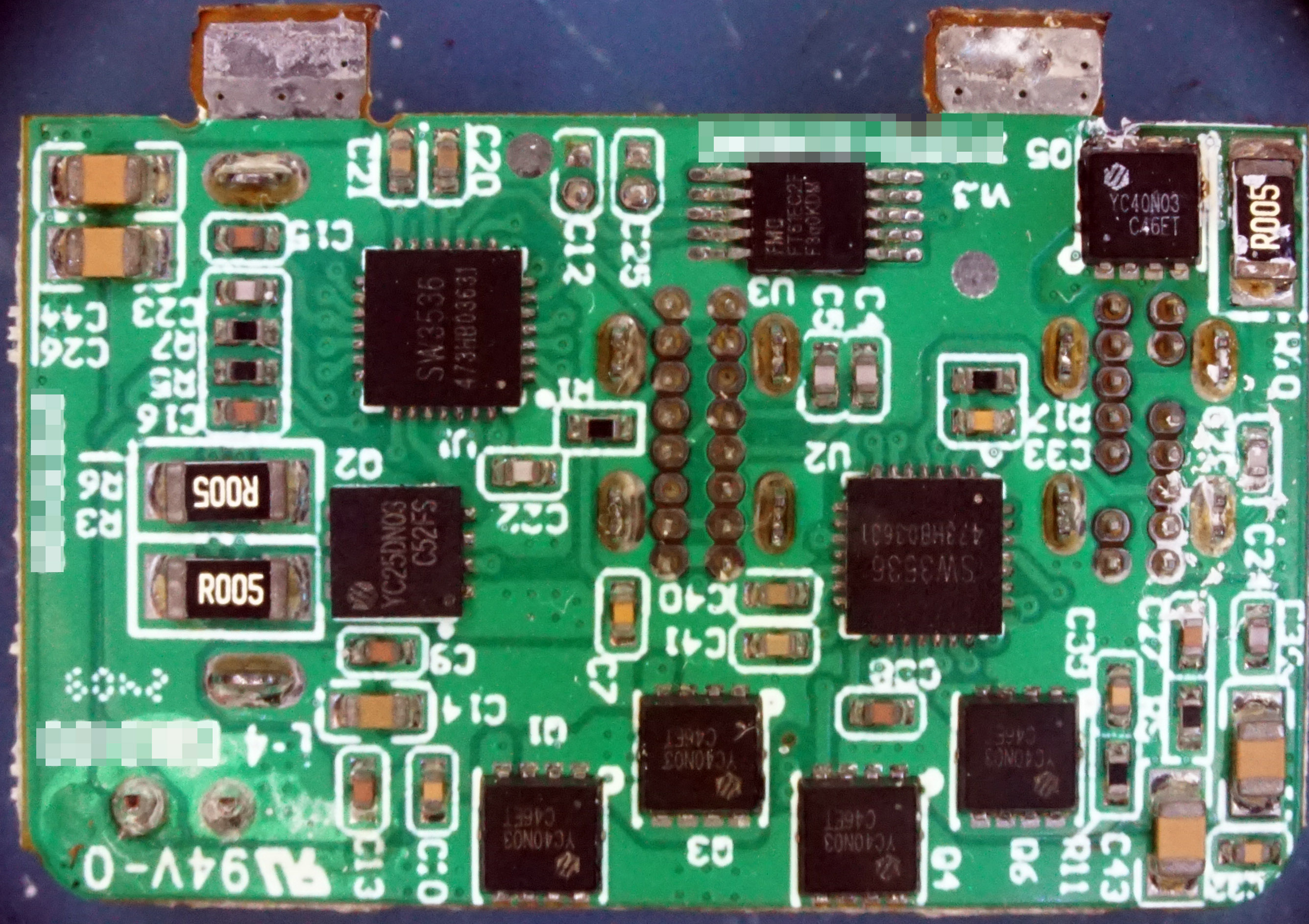
The Ware for March 2025 is shown below.
I was just taking this thing apart to see what went wrong, and thought it had some merit as a name that ware. But perhaps more interestingly, I was also experimenting with my cross-polarized imaging setup.
This is a technique a friend of mine told me about where you put a polarizer on the light source, and then put another polarizer 90 degrees from the light source in front of your imaging lens. As you can see from the comparison above, the contrast on the part numbers is greatly enhanced — at the expense of losing most of your light. What isn’t obvious from the two images is the one on the left required a much longer exposure because 90+% of the light is not reaching the camera due to the cross-polarization.
My understanding of the theory is that with this technique, light that hits textured surfaces is more scattered (and likewise the polarization is more randomized) by the rougher, laser-marked regions of a chip label, while light bouncing off of smoother surfaces is attenuated because the polarization is more preserved (and thus blocked by the cross-polarized filter on the lens). So it’s less of an enhancement of the laser marked regions and more of an attenuation of everything that’s not.
The solution to the attenuation problem in our modern era is to just throw more light at it and mount your camera on a stand so you can afford a longer exposure time. Fortunately white LEDs are really cheap and ridiculously powerful, and I have some extra COB-based ring light emitters laying around the lab. The technique doesn’t scale to large boards as easily, but it just so happens this particular ware fits nicely in the field of view of the illuminator + camera.
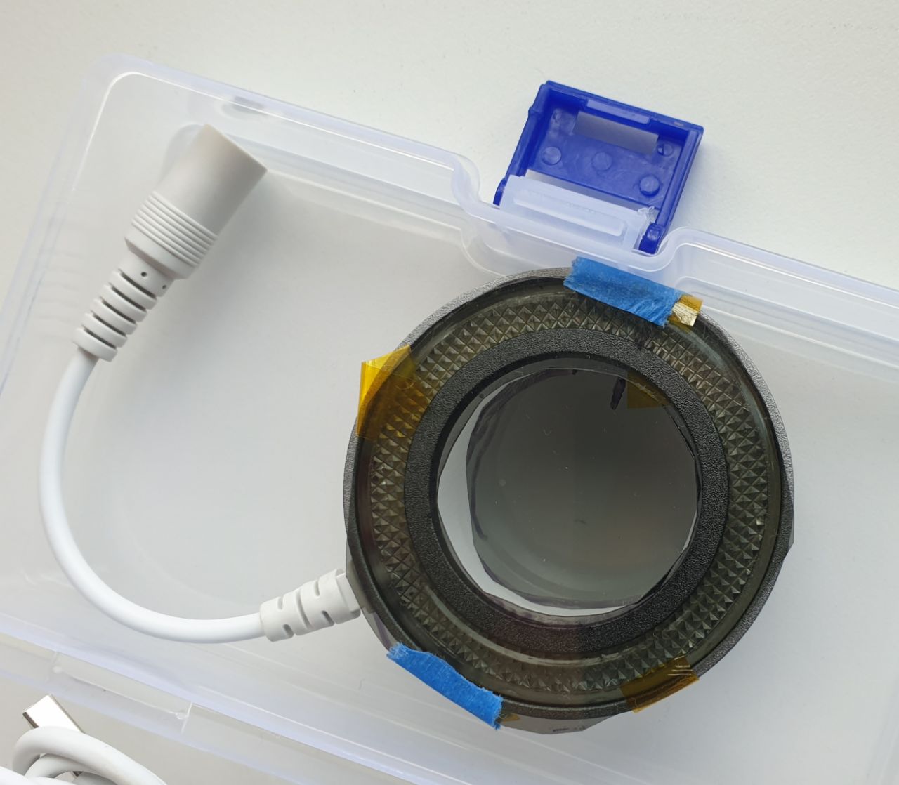
The whole setup is pretty crude…just a cheap polarizer film that was rough-cut with scissors, and taped onto a $10 COB ring light I picked up some time ago in the Shenzhen markets that screws directly into the accessory threads of the objective on my benchtop microscope. Works OK, tho!
I’ll guess that this is some sort of USB charger. SW3536 seems to be a PD/PPS protocol IC. YC40N03 and YC25DN03 seem to be MOSFETs but cannot find their datasheet.
A few other observations: there are 2 SW3536 protocol ICs and 2 USB C ports (those through hole parts should be USB C connectors). Funny thing is they’re using different footprints, one of them have 2 pins missing. My guess would be that these are SBU pins as CC pins are needed for PD and I can see the CC2 pin of the left SW3536 and CC1 pin of the right SW3536 connected to the pins (3rd from top and 3rd from bottom respectively).
10 pin component at the very top is a FT61EC2 MCU in MSOP10 package. Probably used for managing everything.
USB backup battery/power pack?
Maybe the big solder tabs at the top of the picture connect to the battery.
Several MOSFETs to control the various charge/discharge paths.
Something seems off for the USB charger idea. Why are the USB-C ports mounted 90 degrees from the board? Don’t most chargers have them out the side/end? You’d expect them to lie parallel to the board then.
And the different kind of USB-C jacks is strange. From a cost reduction standpoint, using two of the same part makes more sense then using two similar but different parts. Even if you don’t need the two missing pins, using two of the same part should more than offset the cost difference.
Those tabs clearly look like they solder into slots into another board–maybe the mains board that takes AC and converts it to DC, but there should be some signaling to say what voltage it needs.
Also, what’s the out of focus thing on the lower left? Looks like two pins/wire/leads that head up off the board.
Found it — spoilers! This is a G651A2CK “65W GaN Pro Fast Charger” from “Rocoren,” though the actual manufacturer is “Shenzhen Goodwin Technology Co. Ltd.” As far as I can tell this model isn’t sold in the USA anymore, and Rocoren seems to have removed its listing page from their site. The fact that Shenzhen Goodwin has no UL Product iQ or FCC listings with any model numbers related to this device might suggest why that’s the case.
There are some good hints to the board’s purpose here: On the board we see two SW3536 USB-PD controller IC’s manufactured by “iSmartWare”. These operate as buck converters and support a comically-long list of USB charging protocols. No buck/boost feature on those IC’s, though. For that matter, no battery safety features visible anywhere on the board either, so we’d have to be missing a lot of stuff for this to be part of a battery bank. There’s also a microcontroller managing everything, a neat little 8-bit RISC Fremont Micro Devices FT61EC2F chip that completely distracted me. The two THT solder points visible on the left side of the image are exactly spaced for a USB-A port, so we’re looking at a device with USB-A + dual USB-C. I’ve seen a lot of wall power adapters with that arrangement, it’s similar to the adapter I use for my Pinecil soldering irons (it’s possible that’s how this particular device was being used when it met its untimely end). The 94V-0 silkscreen in the bottom-left of the board is a V-0 flame retardant rating, which I believe is a requirement for UL testing of anything wall-powered, too. There’s also a nice radius on the bottom two corners of the PCBA which isn’t present on the top, suggesting that this board might be meant to fit into an enclosure with rounded corners. All together, we’re probably looking for a wall power adapter with USB-A and dual USB-C ports.
Unfortunately, I’ve found out there are an awful lot of wall power adapters with USB-A and dual USB-C ports. Luckily for me, the mystery FETs “YC40N03” and “YC25DN03” led me home here. Googling those two part numbers leads to two different places: This NTW post, and some AliExpress links for the G651A2CK power adapter. That power adapter is already a really good match since it exactly fits the shape & size of this board, but digging around those AliExpress links gave me no clues as to why those two FET part numbers had led me there. Maybe someone had put it in a review that was later deleted? I spent a long time trying every possible way to get internal photos of that power adapter, to no avail — no FCC or UL listings to be found. Finally I clicked on one of the links to the Russian-language AliExpress site, which led to a review from one Ukranian guy “Olexandr U.”. Thank you Olexandr, your review goes into more engineering detail than any power supply review I have ever seen and contains gorgeous photos of every internal circuit in this adapter, including the exact board that we’re looking at here. The two solder tabs on the top of the board solder into another PCBA that contains all of the AC conversion circuitry for the wall adapter, which then feeds something like 20VDC into the pictured PCBA.
And Bunnie — Are you sure you want to repair this wall adapter? Olexandr was able to find an Intertek 62368-1 listing for this device, but it also apparently has no thermal protection at all.
I think I found the same AliExpress link when I was searching those part numbers. But I dismissed that link as I couldn’t find the comment that mentions the part numbers at the time. I believe the link to this post is due to my initial comment. :D
Good catch on the USB A port! I dismissed those as board-to-board or board-to-cable connectors as I couldn’t see the solder points for the pins themselves. Managed to find the reviews. And man those pictures are something! I was guessing the top solder pads as power input but I never imagined that this board is soldered to another board at a right angle, that’s an interesting build. The lower left pins seem to be connected to a through hole capacitor. I wonder why they did this as there seems to be an SMT cap with the same values on the same side.