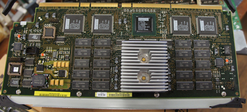
The Ware for September 2011 is a DEC Alpha 21164A microprocessor board. This is a product from circa 1996: a 64-bit CPU that ran from 366-666 MHz, fabricated in 0.35um technology with a Vdd of 2.5V, and featured a discrete L3 cache with five support chips. Back in the day, having one made you the coolest kid on the block. Chicks would come by just to watch how fast gcc would spit out object files while compiling the kernel (ahem, I did go to a nerd school). Contrast today to an Intel i7-2600k that runs four cores between 3.4-3.8 GHz, fabricated in 0.032um (32nm), a Vdd of ~1.25V, and integrates the memory controller, graphics controller, 8MB of L2 cache, and other goodies. If you could warp one back in time to 1996 it would almost be alien technology.
I’m still fond of the Alpha, it has a very “clean” architecture that was great for learning and teaching. I still remember the headlines about Alpha breaking the 5V barrier and using a 3.3V power supply. There were a lot of articles in the trade magazines (they didn’t have blogs back then!!) trying to explain how and why this is a good thing. When I saw this board laying in a scrap heap, I had to take a photo and share it for old times sake. An easy one to guess, but I have to remember that most college-age students today have never used one, and probably think of it as more an academic curiosity than as a serious machine. Winner is FlorinC for being the first one to guess it. Congrats, email me to claim your prize!
Below is a shot of the board without the redacted part numbers.

awesome stuff; back in the days over here in europe you’d only get hold of that kind of hardware when working for financial insitutions (which I luckily did).. sweet hardware, awesome Operating Systems ..
Is the checkerboard pattern in the top metal layer EMI related, or just for kicks?
Checkerboard pattern is to equalize the amount of copper that’s being etched off the layer. As the copper dissolves into the etchant it can cause a localized dilution of active etchant and slowing of the etching rate; so if you have big regions without copper you can get under-etching in adjacent traces that can cause thin traces to become fatter.
It’s probably also useful on inner layers of multi-layer stacks to prevent “sinkage” because with very thin dielectrics the thickness of the copper becomes significant compared to the dielectric, and as you create the sandwich you’ll get sunken regions; the dummy copper helps maintain a uniform average density. But I think the primary reason is for etchant consumption equalization.
These days I think board houses have new techniques that don’t require this sort of equalization, it’s rare to find someone who imposes a copper density design rule. I don’t know what process improvement has been done to avoid this, but I’m guessing they are either doing a spray-etch or have found ways to agitate the fluid so that the panels aren’t sitting in a roughly static bath of etchant. Or they have gotten really sophisticated and they have CAD tools that can pre-compensate the artwork for over/under etching depending upon local pattern densities.
seo…
[…]Winner, Name that Ware September 2011 « bunnie's blog[…]…