HackDAC Theory
In order to understand how to build your own A/D converter, I’d like to take this chance to talk a little bit about the theory behind analog and digital signals, and give a little background behind what an A/D converter is.
Background
Just what is a digital signal? The pedestrian visualization of a digital signal is something akin to a stream of 1 and 0 characters floating down a pipe. However, in reality, Mother Nature knows no 1’s or 0’s. Abstract concepts, such as the binary digit, must eventually manifest themselves as measurable, observable parameters. A piece of digital information is ultimately converted into a measurable analog quantity. In other words, at some point a bit turns into an electromagnetic perturbation—such as a voltage or a current, or photonic intensity—that is vulnerable to the natural entropic processes that degrades data.
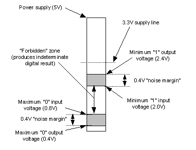
The digital secret sauce is how these analog quantities are interpreted. This interpretive process is codified by a signaling convention (also referred to as the “physical layer specification” in more complex schema); there are many signaling conventions, each of them trading off robustness, power, bitrate and information density for a specific application. These conventions maybe as simple as the old signal amplitude based TTL signaling convention, or complex like the OFDM (Orthogonal Frequency Division Multiplexing) standards used in WiFi (802.11g) and many terrestrial cable modem standards. Regardless of the details, all digital conventions feature the restorative property: the amplitude of a signal output must be larger than the minimum detectable signal input. In other words, a guard band for noise must be provided between the transmitter and the receiver. For example, Figure 1a illustrates what the old TTL convention looks like. Here, a digital “1” is understood to be an analog voltage above a value of 2.0V, and a digital “0” is understood to be an analog voltage below 0.8V. Significantly, any TTL-compliant device must output a margined voltage, e.g., a digital “1” output must be 2.4V or greater. Thus, the signal can encounter over 0.4V of noise before it becomes illegible as representing a digital “1”. One can see plainly here the restorative property of this standard: a TTL driver may output 2.4V, and even though a receiver can see this same signal with an amplitude as small as 2.0V after noise impairments, the receiving buffer must restore the analog quantity to a value back above 2.4V before passing it onto the next logic stage.

Figure 1a: Diagram of signaling convention for the old TTL standard, based on 5V logic. Note the relative inefficiency of this standard, with a very large positive voltage margin available above the minimum “1” output voltage. Note that there is little coincidence that CMOS gates on a 3.3V supply line is directly input-compatible with this standard.

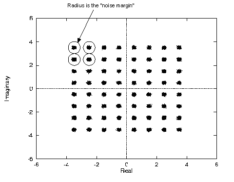
Figure 1b: Diagram of a 64-QAM OFDM (Quadrature Amplitude Modulation Orthogonal Frequency Division Multiplexing) “constellation”. In this complex signaling standard, information is represented by a combination of phase and amplitude. You may recall from geometry that sines and cosines can be represented as a sum of exponentials with “imaginary” components. These imaginary components in effect keep track of the phase information in a signal, and signal designers use this extra phase dimension to increase the efficiency of their signaling standards. A convenient representation of these real-versus-imaginary signals is the constellation plot, where a polar radius, as opposed to a linear scale in amplitude-only signaling schemes, represents the noise margin. Interestingly, the time-domain waveform of an OFDM signal looks nothing at all like what one might expect for a digital signal. The signal is actually rather noise-like, a sign of high bandwidth efficiency from an information theoretical standpoint. This is where the lunatic fringe of digital signaling meets the real analog world.
The subject of just how much noise guard band is required is a fascinating one. As we continue to push the boundaries on information density and bitrates, the tricks we play to make digital signals work are starting to break down—digital technology is on the verge of coming out of the analog closet. At very high signal speeds or densities, there is an important energy-time trade-off that digital signal designers must consider. The faster/denser you send/store bits, the less energy and time are available to interpret the information. In fact, the term Bit Error Rate (BER) is starting to appear more and more in product literature. BERs are typically specified in terms of expected failures per bits transmitted. For example, a brand-name hard drive today has a non-recoverable error rate of 1 per 1014 bits—in other words, once every 12,500 Gbytes transferred. This state of the art hard drive today stores 500 Gbytes of data. Chew on this: if you were to read data off of this drive continuously, you should expect an unrecoverable bit error just once every 25 times through the entire drive’s contents. Another way of looking at this is one in 25 hard drives performing this experiment should expect a bit error after one complete beginning to end read pass . Feel worried about the integrity of your data yet? Don’t look now. Hard drives encode data so densely that quite often there is insufficient energy stored in a bit to detect the bit on its own, so hard drives use Partial Response, Maximum Likelihood (PRML) techniques to recover your data. In other words, the hard drive controller looks at a sequence of sampled data points and tries to guess at what set of intended bits might have generated a particular response signature. This technique is combined with others, such as error correction techniques (in itself a fascinating subject), to achieve the intended theoretical bit error rates. Have valuable data? Become a believer in back-ups. Our robust digital complacency is starting to ooze back into the analog days of pops, clicks and hiss. Bit errors are not confined to storage, either. Many high-speed serial links are specified to perform at BER’s as low as one error per 1012 bits. While error-free enough for a single user to tolerate, these error rates stack on top of each other as you build more complex systems with more links in them, to the point where managing error rates and component failures is one of the biggest headaches facing server and supercomputer makers today.
Analog ex Digita
One can now see, hopefully, that there is no “analog” or “digital” per se in the circuit world, just a set of (arbitrary) rules used to interpret analog values. In reality, every digital gate in a logic system is performing a 1-bit analog to digital conversion. We can exploit this fact to build an analog to digital converters out of nothing but standard digital parts: an FPGA and a handful of 100-ohm resistors. Before we do this, let’s review a little bit of ADC theory first.
From A to D
Building a robust, high-quality and manufacturable Analog to Digital converter is not a trivial subject. Many dissertations and books have been written on the subject, and artisan circuit designers specialize their careers around such a topic. However, many factors have come together to enable ordinary hackers like you and me to build basic video-rate data converters. We’ll explore the bare minimum theory necessary to understand this subject before diving into the practical example.
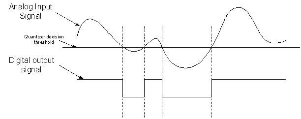
The heart of every analog to digital converter is a device called a quantizer. A quantizer takes an analog voltage or current, compares it against a set of well-defined thresholds, and outputs a digital code based upon the comparison. The simplest quantizer is a 1-bit comparator: if a voltage is above a certain threshold, a “1” is output; below that threshold, a “0” is output. Figure 3 illustrates how this quantizer might operate on an analog signal. As mentioned previously, every digital gate is in its own right a comparator, although digital gates exhibit some properties that can interfere with high-quality operation, such as hysteresis.

Figure 3: Operation of the 1-bit quantizer. An analog input is “sliced” along a decision threshold into voltages that represent digital-signaling convention compliant 1’s and 0’s.
Quantizers can also be multi-bit, in the sense that they can take in an arbitrary analog voltage and attempt to resolve the voltage to an N-bit code. Typically, one strives to design this quantizer so that every valid N-bit code corresponds to an evenly distributed set of analog voltages across a certain linear range of values. Thus, a 16-bit quantizer must be able to resolve a voltage input into one part in 65,536 (= 216). At an input level of 1 volt, that corresponds to a resolution of better than 0.000015 volts, or 15 micro-Volts. Achieving this level of precision is a major challenge, especially at a high conversion rate. To give a sense of scale for the difficulty of this problem, a 1.4k-ohm resistor generates about 15 micro-Volts of thermal noise at room temperature over a 10 MHz bandwidth. This thermal noise, also known as Johnson noise, is due simply to the thermally agitated Brownian motion of charges within a resistor, and like the speed of light, there is nothing you can do about it.
Allow me to take this paragraph to digress for a moment. The applications of linear 16-bit quantizers are ubiquitous—recall that CD-quality audio uses samples with at least 16 bits of resolution. How is it that digital audio is so pervasive, yet so challenging to manufacture? A very clever technique, known as sigma-delta conversion, uses cheaper quantizers of reduced precision along with oversampling techniques to create a virtual high-resolution output. Most digital audio products today in fact use this technique. Wrap your head around this: sigma-delta converters treat the inherent error of using a reduced-precision quantizer as “noise”, and they use a set of filters (typically implemented in the digital domain) to spectrally shape this noise so that it is outside the bandwidth of interest. It is kind of like being able to choose where you make your mistakes, so that they don’t matter as much. This is a marriage made in heaven for Moore’s Law: the flaws of sloppier (and more manufacturable) analog quantizers are corrected by throwing gobs of digital logic at the problem. CMOS logic is getting faster, cheaper, and smaller at an exponential rate, and this style of data converter is in a unique position to benefit from this trend. This fact alone should get your hardware hacker gears turning in your head—Field Programmable Gate Arrays (FPGAs) offer hackers a plethora of cheap, flexible digital logic, and as mentioned previously, 1-bit quantizers (e.g., any digital input). This is a situation ripe for the home-brew of audio-quality data converters, should the RIAA ever attempt to implement its version of the watermark detectors on audio-rate data converters.
The chief disadvantage of sigma-delta converters (also called 1-bit converters, because they are often implemented using a 1-bit quantizer) is that their conversion rate is limited due to their use of oversampling. In other words, sigma-delta converters can be used for CD-quality audio because samples trundle along at a leisurely 44.1 kHz, whereas in digital video, samples need to be taken at rates often exceeding 1,000 times audio rates. When it comes to doing video, there is one classic data converter implementation that comes to my mind: the “Flash” data converter. The “Flash” term comes simply from the fact that it is one of the fastest data converter implementations; it has nothing to do with the FLASH memories that are used in your solid-state USB disk fobs or camera CF cards.
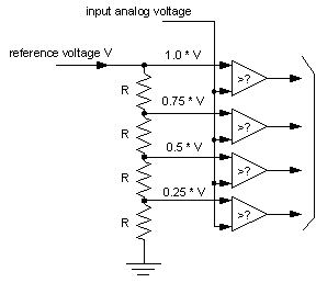
Flash data converters are the simplest and perhaps the fastest multi-bit quantizer implementations. The heart of a Flash analog to digital converter is a set of resistors strung together in series. This so-called resistor ladder equally divides an input voltage across each resistor. Thus, a 1-volt input across a 4-resistor ladder will result in 0.25 volts developing across each resistor (see Figure 2). An input analog voltage can then be compared in parallel against this reference voltage ladder using an array of 1-bit quantizers. The resulting digital output is coded in a form called a “thermometer code”, where the output value is equal to the length of consecutive 1’s in the code. So in this example:
binary		thermometer
00		0000
01		0001
10		0011
11		0111
*		1111   [overflow condition]

Figure 4: The basic Flash A/D converter core.
This converter is extremely fast because the entire conversion happens in a single wide parallel conversion operation, as opposed to the sigma delta/oversampled or successively approximated methods used in other converters. This architecture has some significant drawbacks, however, including:
The good news for us is two-fold: first, the human eye is remarkably insensitive to quantization artifacts. The “True Color” mode on your graphics card uses 8 bits per color channel. The human eye is particularly insensitive to quantization artifacts in bright areas, so much of the color depth goes toward reducing “banding” effects in low-light level or darker areas. The other good news is that the basic Flash A/D converter core can be combined with other techniques, such as oversampling, pipelining, folding, and re-sampling, to achieve a compromise solution that balances complexity against performance.
Do you mind if I quote a couple of your articles as long as I provide credit and sources back to your blog: http://www.bunniestudios.com/blog/?page_id=22. I’m going to aslo make sure to give you the proper anchortext link using your blog title: HackDAC Theory bunnie's blog. Please make sure to let me know if this is acceptable with you. With thanks
Yes, that’s fine.
What about a unique take on the successive approximation method where ‘n’ quantizers are used? Vref of each lower bit selected from a bank of 2^n possible two resistor dividers dictated by the previous result of the more significant bit.
This would eliminate the resistor matching issue and only require ‘n’ quantizers. Speed would be less, but orders of magnitude faster than a traditional sample-hold SAR method.
It’s something I have been toying with trying out once I get more familiar with FPGAs.
I have seen a similar idea to your flash A/D circuit used for sample/hold circuits which were in turn being used to measure the time taken for light pulse to travel a variable distance. As you pointed out, high-precison is a casualty but the response was fast.