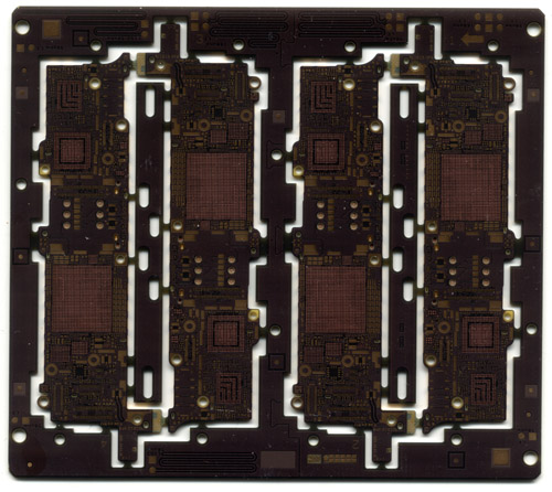
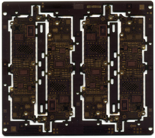
The Ware for June 2013 is shown below.
This month we’re fast-forwarding 25 years and having a look at another high density signal interconnect, but of a different nature — should be a walk in the park to guess it.
I find it interesting that the BGA/QFN regions use OSP (organic solder preservative, you can tell from the brownish color of the BGA regions), whilst the rest of the pads employ a gold finish. It’s also neat to see the impedance test coupons around the edge of the frame. And the partial/blind mounting holes through the board? Yeesh, talk about scrounging for millimeters.
Also, not a single bit of silkscreen, nor any proprietary notices or trademark/copyright claims, even on the frame. Interesting.


Nice peace of hardware there, I’m guessing a ton of burried vias, and a very expensive PCB…
1292 pads BGA in the center, not a rectangular PCB, with RF and differential signals.
As it seems too large to fit in a smartphone, and don’t see RAM BGAs, I’ll go for a smartbook motherboard.
Ram chip can be stacked on top of the CPU.
Never cranked open an iphone5 yet, but yes as mentioned by ifixit, the A6 chip has an LPDDR2 POP package on top of the processor.
Seen this on OMAP4430 on one of our board, but the OMAP4430 was not as big as the A6…
So iphone5 logic board it is.
Hi,
It seems to be a phone board, with the SIM connector and so on…
The BGA is very large, a 34×38 matrix.
I’ve only seen this matrix in the Apple A6 processor.
Looking for the iphone 5 logic board, I’ve found this pictures that is identical to the image shown:
http://www.aliexpress.com/item/For-iphone-5-Motherboard-logical-board-mainboard-bare-board-not-accessories-free-shipping/679983379.html
The new iphone 5s board leaked is a bit different.
Regards,
mangel
yep, definitely looks like an iPhone 5 PCB (clone?)
http://www.ifixit.com/Teardown/iPhone+5+Teardown/10525/2#s38293
yes I think it’s a clone – see my link below
It is the real iphone 5 mainboard.
Here it is the iphone 5 assembly drawing
https://anonfiles.com/file/745666317776b454b672189cb27a5cdc
Nope, that’s the motherboard from an iPhone 5S.
Too slow, and wrong to boot.
Ignore me, please.
How many copper layers could you pack on such a design? 8? 12?
I see an impedance test on layer 10 – second photo bottom – that is on an internal layer, so probably at least 12 layers.
I guessing the motherboard for a tablet. Is the lack of silkscreen because the process hasn’t run yet, or those boards are just never silkscreened?
“Dummy replacement for iPhone 5 motherboard”:
http://www.alibaba.com/product-gs/955219404/OEM_motherboard_for_iphone_5_Dummy.html
Mangel’s ID of the A6 BGA and conclusion that this must be an iPhone 5 is backed up by a search on the part number visible on what appears to be the camera mounting stub. That yields multiple hits for replacement iPhone 5 16GB main PCBs and images that appear to match.
It’s the new ipad mb! -j
820-3141-b apple iphone 5 main board
iphone 5 it is!
[…] Name that Ware, June 2013. The most interesting thing about bunnie’s june ‘ware of the month’ (its an iPhone 5 board) is the ’50 ohm’ test traces at the outlines of the panel, which look like impedence-testers. cool idea for RF PCB design analysis! […]