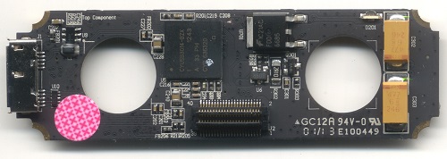
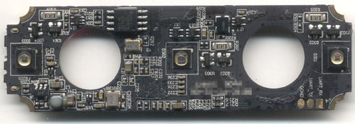
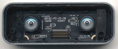
The Ware for September 2013 is shown below.
Just barely made the month of September! It’s been a hectic month, and it looks like I’ll be struggling to keep up for the rest of the year. So many things I’d like to write about, but so little time!
[cat’s out of the bag, so here’s the other views of the ware, for your viewing pleasure]


It’s a Leap Motion Controller
Here’s a photo of the Leap Motion controller for reference:
http://i.imgur.com/sHM4Mxo.jpg
The three high-powered IR LEDs are a good indication that something is being illuminated (Just like the Xbox kinnect) and the large two holes are clearly for housing sensors, in this case two IR cameras that do comparative calculations to form a 3D model (the PCB is far too small to contain a CPU powerful enough to do this, I assume this is calculated on the PC, to save on installing a large RISC processor or some kind of FPGA,it would also make it cheap too.).
It’s the CCA from a Leap Motion controller. BTW Tales from Shenzhen at Maker Faire was awesome one of the only talks I made sure I saw while I was there.
thanks!
Found a nice teardown while searching for more pictures: https://learn.sparkfun.com/tutorials/leap-motion-teardown/all
(very interesting: there is no MCU/CPU on the board at all!)
obligatory ifixit: http://www.ifixit.com/Teardown/Leap+Motion+Controller+Teardown/14213/1
There is an MCU on the board, but it’s on the back side…I left the back-side view out of the contest photos to try to make it more difficult…but apparently, it still wasn’t hard enough. I’ll try to post photos of the reverse side with the micro on it later on.
The Sparkfun guy said it was a USB 3.0 controller, not an MCU.
But you’re right http://www.cypress.com/?docID=44322 – its a USB 3.0 controller with a ARM926EJ core. So it does have a CPU.
The name of the bottom jpg gave a little hint too: leap_bottom.jpg
Correct, I posted that photo in an update after it was guessed…no need to obfuscate names anymore!
Yeap! Leap motion controller
Leap! All of the earlier dev units were sent out caseless, so I imagine that PCB shape + the LEDs (not necessarily the rest of the circuit… it’s a lot more complicated now) are pretty familiar in the dev community by now :)
I’m also curious what you thought of the device itself!
Any clue why L1 and L2 have epoxy or potting?
My guess: epoxy glue to avoid damage if the device receives a shock.
These are “heavy” SMD components that could end unsoldered (or harmed) if the device falls on the ground from some height.
Magnetic components can also vibrate and fail. But I doubt this is the case on a properly designed switching psu.