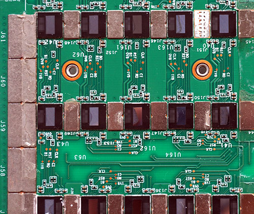
The Ware for June 2024 is shown below.

This one will probably be a super-easy guess for some folks, but the details of the design of this type of ware are interesting from an engineering standpoint. Some of the tricks used here are kind of mind blowing; on paper, I wouldn’t think it would work, yet clearly it does. I’ll go into it a bit more next month, when we name the winner. Or, if you’re already an expert in this type of ware and have circuit-level insights to share, be my guest!
With what looks like a large number of exposed dies, connected serially with 0.8 and 1.8v supplies and a considerable amount of ground-plane heatsinking? I’m going to guess this is part of a gigapixel sensor array, possibly as used in large optical telescopes? a copy of the image is cast onto each die, and because of the lenses being in slightly different positions, you can combine the images to have much higher resolution than the underlying sensors. I’ve never seen inside one of these, if that’s what it is! :)
Large array of chips, essentially no I/O except CLK/CI/BI/RO/RST serial bus… and that doesn’t look like it’s a fast one. Given the attention to heat dissipation (the metal spacer blocks, custom exposed-die packages) I’m going to guess those chips are doing a lot of compute while communicating very little with the outside world. About the only use case I can see for that is some sort of coin miner, probably Bitcoin… scientific parallel calculation stuff tends to need way more bandwidth and (at least virtual) full connectivity between chips, yet the bus is clearly linear (and probably linear if it’s a miner)…
bitcoin miner
chips powered in series
You’re right. It’s this one: https://antminer-repair.com/products/antminer-s19j-pro-board-repair
I’m not an electronics engineer, but the one part that strikes me as “cannot possibly work” is power supply. 1.8V is presumably IO and thus low current, but 0.8V smells like Vcore, with associated multi-amp power draw… yet it doesn’t seem to be connected to anything? So either there’s plenty of vias hidden underneath the package, or it’s a weird design of some kind.
Maybe the chips really just have the power connections in series, and have enough margin that the ones closer to the end of the trace simply work at way lower Vcore? The chips do look like they are designed with feed-through layout for not just signals but also power. Miners probably run each individual chip at the highest frequency that this particular chip can handle with an acceptable margin for error, so an underspec Vcore would simply result in slightly lower overall performance.
Given that the chips are labeled all over the place (U41 is next to U162, but U42/U43 are just randomly on the other side of the photo), my guess is that they simply churned out that board as fast as possible to be first to market and in quantity… I do remember reading a story about a crypto chip design that was the designer’s first chip ever, but had to be taped out untested in the millions because waiting and testing would have negated its performance lead. So maybe slightly lower efficiency was simply worth having the hardware out a few weeks before the competition?
It looks like it may be a BHB68xxx mining board.
Those are Hashing ASICs which are wired powered by big 1.2V and 0.8V busses. They are wired serially across the board with the RST/CLK/RI/RO/CI/CO signals. Those copper slugs (one missing between U40 and U163) are used to conduct heat between the ground plane and the heatsink. They also have better conductivity than the PCB so they act to enhance its current carrying ability.
The individual ASICS are wired in series and the board is fed from a controller board which typically consists of an FPGA which can drive many of these long serial chains at high speed. The controllers often use FPGAs with built in CPU cores which run the mining controling software and host a web interface for the mining control software/user to use to coordinate mining activities amongst mining assemblies.
The specific board will be hard to find because these machines were itterated on very quickly as improvements in mining ASICs came out which obsoleted older boards because it was always a race between power efficiency vs mining rate vs the current value of the hashing work. But as the value fluctuated up and down older machines would be brought back into service if they again became proffitable–which lead to a large secondary market for the devices and the associated repair industry.
The chips are likely the BM1368. I assume that’s the part that’s been blurred off.