Author Archive

Winner, Name that Ware March 2024

Tuesday, April 30th, 2024

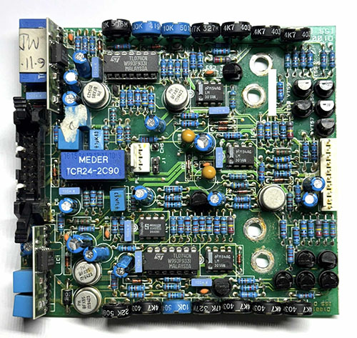
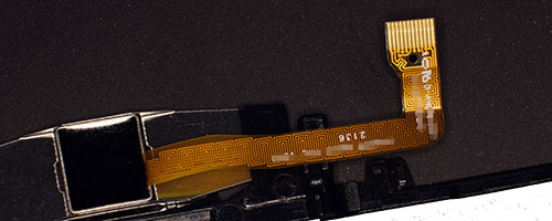
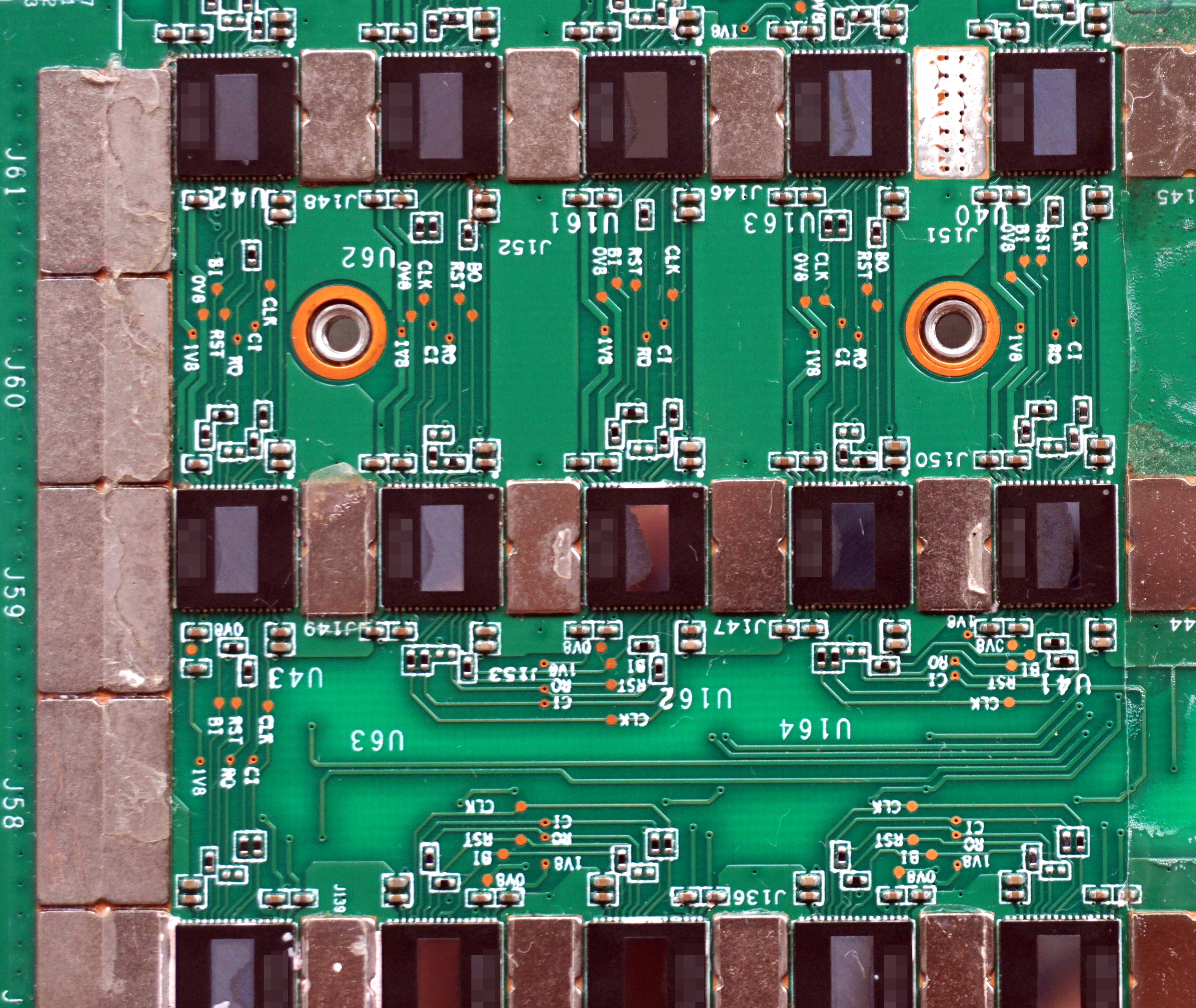
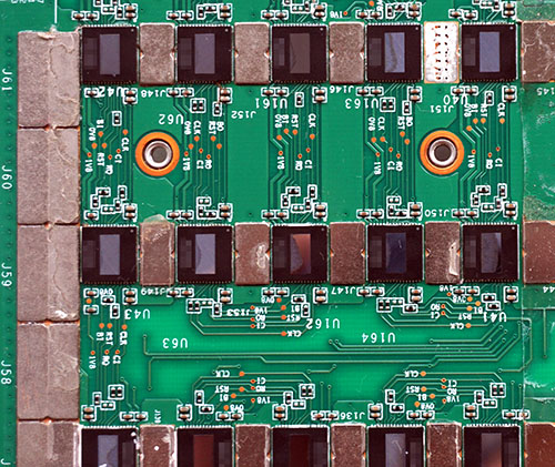
Last month’s ware was internals from a VCH-1006 passive hydrogen maser. KE5FX has published a great write-up about the unit, its history, and how it was repaired.

I’ll give the prize to Hessel. The guess given was about as close as anything I could have done myself — a pretty challenging ware, as I’ve never seen anything quite like this before. Congrats, email me for your prize!

Automated Stitching of Chip Images

Monday, April 22nd, 2024

This is the final post in a series about non-destructively inspecting chips with the IRIS (Infra-Red, in-situ) technique. Here are links to previous posts:

This post will cover the software used to stitch together smaller images generated by the control software into a single large image. My IRIS machine with a 10x objective generates single images that correspond to a patch of silicon that is only 0.8mm wide. Most chips are much larger than that, so I take a series of overlapping images that must be stitched together to generate a composite image corresponding to a full chip.

The un-aligned image tiles look like this:

And the stitching software assembles it into something like this:

The problem we have to solve is that even though we command the microscope to move to regularly spaced intervals, in reality, there is always some error in the positioning of the microscope. The accuracy is on the order of 10’s of microns at best, but we are interested in extracting features much smaller than that. Thus, we must rely on some computational methods to remove these error offsets.

At first one might think, “this is easy, just throw it into any number of image stitching programs used to generate panoramas!”. I thought that too.

However, it turns out these programs perform poorly on images of chips. The most significant challenge is that chip features tend to be large, repetitive arrays. Most panorama algorithms rely on a step of “feature extraction” where it uses some algorithms to decide what’s an “interesting” feature and line them up between two images. These algorithms are tuned for aesthetically pleasing results on images of natural subjects, like humans or outdoor scenery; they get pretty lost trying to make heads or tails out of the geometrically regular patterns in a chip image. Furthermore, the alignment accuracy requirement for an image panorama is not as strict as what we need for IRIS. Most panaroma stitchers rely on a later pass of seam-blending to iron out deviations of a few pixels, yielding aesthetic results despite the misalignments.

Unfortunately, we’re looking to post-process these images with an image classifier to perform a gate count census, and so we need pixel-accurate alignment wherever possible. On the other hand, because all of the images are taken by machine, we never have to worry about rotational or scale adjustments – we are only interested in correcting translational errors.

Thus, I ended up rolling my own stitching algorithm. This was yet another one of those projects that started out as a test program to check data quality, and suffered from “just one more feature”-itis until it blossomed into the heaping pile that it is today. I wouldn’t be surprised if there were already good quality chip stitching programs out there, but, I did need a few bespoke features and it was interesting enough to learn how to do this, so I ended up writing it from scratch.

Well, to be accurate, I copy/pasted lots of stackoverflow answers, LLM-generated snippets, and boilerplate from previous projects together with heaps of glue code, which I think qualifies as “writing original code” these days? Maybe the more accurate way to state it is, “I didn’t fork another program as a starting point”. I started with an actual empty text buffer before I started copy-pasting five-to-twenty line code snippets into it.

Sizing Up the Task

A modestly sized chip of a couple dozen square millimeters generates a dataset of a few hundred images, each around 2.8MiB in size, for a total dataset of a couple gigabytes. While not outright daunting, it’s enough data that I can’t be reckless, yet small enough that I can get away with lazy decisions, such as using the native filesystem as my database format.

It turns out that for my application, the native file system is a performant, inter-operable, multi-threaded, transparently memory caching database format. Also super-easy to make backups and to browse the records. As a slight optimization, I generate thumbnails of every image on the first run of the stitching program to accelerate later drawing operations for preview images.

Each file’s name is coded with its theoretical absolute position on the chip, along with metadata describing the focus and lighting parameters, so each file has a name something like this:

x0.00_y0.30_z10.00_p6869_i3966_t127_j4096_u127_a0.0_r1_f8.5_s13374_v0.998_d1.5_o100.0.png

It’s basically an underscore separated list of metadata, where each element is tagged with a single ASCII character, followed by its value. It’s a little awkward, but functional and easy enough to migrate as I upgrade schemas.

Creating a Schema

All of the filenames are collated into a single Python object that tracks the transformations we do on the data, as well as maintains a running log of all the operations (allowing us to have an undo buffer). I call this the “Schema” object. I wish I knew about dataframes before I started this project, because I ended up re-implementing a lot of dataframe features in the course of building the Schema. Oh well.

The Schema object is serialized into a JSON file called “db.json” that allows us to restore the state of the program even in the case of an unclean shutdown (and there are plenty of those!).

The initial state of the program is to show a preview of all the images in their current positions, along with a set of buttons that control the state of the stitcher, select what regions to stitch/restitch, debugging tools, and file save operations. The UI framework is a mix of PyQt and OpenCV’s native UI functions (which afaik wrap PyQt objects).

Above: screenshot of the stitching UI in its initial state.

At startup, all of the thumbnails are read into memory, but none of the large images. There’s an option to cache the images in RAM as they are pulled in for processing. Generally, I’ve had no trouble just pulling all the images into RAM because the datasets haven’t exceeded 10GiB, but I suppose once I start stitching really huge images, I may need to do something different.

…Or maybe I just buy a bigger computer? Is that cheating? Extra stick of RAM is the hundred-dollar problem solver! Until it isn’t, I suppose. But, the good news is there’s a strong upper bound of how big of an image we’d stitch (e.g. chips rarely go larger than the reticle size) and it’s probably around 100GiB, which somehow seems “reasonable” for an amount of RAM to put in one desktop machine these days.

Again, my mind boggles, because I spend most of my time writing Rust code for a device with 16MiB of RAM.

Auto Stitching Flow

At the highest level, the stitching strategy uses a progressive stitch, starting from the top left tile and doing a “lawn mower” pattern. Every tile looks “left and up” for alignment candidates, so the very top left tile is considered to be the anchor tile. This pattern matches the order in which the images were taken, so the relative error between adjacent tiles is minimized.

Before lawn mowing, a manually-guided stitch pass is done along the left and top edges of the chip. This usually takes a few minutes, where the algorithm runs in “single step” mode and the user reviews and approves of each alignment individually. The reason this is done is if there are any stitching errors on the top or left edge, it will propagate throughout the process, so these edges must be 100% correct before the algorithm can run unattended. It is also the case that the edges of a chip can be quite tricky to stitch, because arrays of bond pads can look identical across multiple frames, and accurate alignment ends up relying upon random image artifacts caused by roughness in the die’s physical edges.

Once the left and top edges are fixed, the algorithm can start in earnest. For each tile, it starts with a “guess” of where the new tile should go based on the nominal commanded values of the microscope. It then looks “up” and “left” and picks the tile that has the largest overlapping region for the next step.

Above is an example of the algorithm picking a tile in the “up” direction as the “REF” (reference) tile with which to stitch the incoming tile (referred to as “SAMPLE”). The image above juxtaposes both tiles with no attempt to align them, but you can already see how the top of the lower image partially overlaps with the bottom of the upper image.

Template Matching

Next, the algorithm picks a “template” to do template matching. Template matching is an effective way to align two images that are already in the same orientation and scale. The basic idea is to pick a “unique” feature in one image, and convolve it with every point in the other image. The point with the highest convolution value is probably going to be the spot where the two images line up.

Above: an example of a template region automatically chosen for searching across the incoming sample for alignment.

In reality, the algorithm is slightly more complicated than this, because the quality of the match greatly depends on the quality of the template. Thus we first have to answer the question of what template to use, before we get to where the template matches. This is especially true on chips, because there are often large, repeated regions that are impossible to uniquely match, and there is no general rule that can guarantee where a unique feature might end up within a frame.

Thus, the actual implementation also searches for the “best” template using brute-force: it divides the nominally overlapping region into potential template candidates, and computes the template match score for all of them, and picks the template that produces the best alignment of all the candidates. This is perhaps the most computationally intensive step in the whole stitching process, because we can have dozens of potential template candidates, each of which must be convolved over many of the points in the reference image. Computed sequentially on my desktop computer, the search can take several seconds per tile to find the optimal template. However, Python makes it pretty easy to spawn threads, so I spawn one thread per candidate template and let them duke it out for CPU time and cache space. Fortunately I have a Ryzen 7900X, so with 12 cores and 12MiB of L2 cache, the entire problem basically fits entirely inside the CPU, and the multi-threaded search completes in a blink of the eye.

This is another one of those moments where I feel kind of ridiculous writing code like this, but somehow, it’s a reasonable thing to do today.

The other “small asterisk” on the whole process is that it works not on the original image, but it works on a Gaussian-filtered, Laplacian-transformed version of the images. In other words, instead of matching against the continuous tones of an image, I do the template match against the edges of the image, making the algorithm less sensitive to artifacts such as lens flare, or global brightness gradients.

Above is an example of the output of the template matching algorithm. Most of the region is gray, which indicates a poor match. Towards the right, you start to see “ripples” that correspond to the matching features starting to line up. As part of the algorithm, I extract contours to ring regions with a high match, and pick the center of the largest matching region, highlighted here with the pink arrow. The whole contour extraction and center picking thing is a native library in OpenCV with pretty good documentation examples.

Minimum Squared Error (MSE) Cleanup

Template matching usually gets me a solution that aligns images to within a couple of pixels, but I need every pixel I can get out of the alignment, especially if my plan is to do a gate count census on features that are just a few pixels across. So, after template alignment, I do a “cleanup” pass using a minimum squared error (MSE) method.

Above: example of the MSE debugging output. This illustrates a “good match”, because most of the image is gray, indicating a small MSE. A poor match would have more image contrast.

MSE basically takes every pixel in the reference image and subtracts it from the sample image, squares it, and sums all of them together. If the two images were identical and exactly aligned, the error would be zero, but because the images are taken with a real camera that has noise, we can only go as low as the noise floor. The cleanup pass starts with the initial alignment proposed by the template matching, and computes the MSE of the current alignment, along with candidates for the image shifted one pixel up, left, right and down. If any of the shifted candidates have a lower error, the algorithm picks that as the new alignment, and repeats until it finds an alignment where the center pixel has the lowest MSE. To speed things up, the MSE is actually done at two levels of shifting, first with a coarse search consisting of several pixels, and finally with a fine-grained search at a single pixel level. There is also a heuristic to terminate the search after too many steps, because the algorithm is subject to limit cycles.

Because each step of the search depends upon results from the previous step, it doesn’t parallelize as well, and so sometimes the MSE search can take longer than the multi-threaded template matching search, especially when the template search really blew it and we end up having to search over a dozens of pixels to find the true alignment (but if the template matching did it’s job, the MSE cleanup pass is barely noticeable).

Again, the MSE search works on the Gaussian-filtered Laplacian view of the image, i.e., it’s looking at edges, not whole tones.

After template matching and MSE cleanup, the final alignment goes through some basic sanity checks, and if all looks good, moves on to the next tile. If something doesn’t look right – for example, the proposed offsets for the images are much larger than usual, or the template matcher found too many good solutions (as is the case on stitching together very regular arrays like RAM) – the algorithm stops and the user can manually select a new template and/or move the images around to find the best MSE fit. This will usually happen a couple of times per chip, but can be more frequent if there were focusing problems or the chip has many large, regular arrays of components.

Above: the automatically proposed stitching alignment of the two images in this example. The bright area is the overlapping region between the two adjacent tiles. Note how there is a slight left-right offset that the algorithm detected and compensated for.

Once the stitching is all finished, you end up with a result that looks a bit like this:

Here, all the image tiles are properly aligned, and you can see how the Jubilee machine (Jubilee is the motion platform on which IRIS was built) has a slight “walk off” as evidenced by the diagonal pattern across the bottom of the preview area.

Potential Hardware Improvements

The Jubilee uses a CoreXY belt path, which optimizes for minimum flying mass. The original designers of the Jubilee platform wanted it to perform well in 3D printing applications, where print speed is limited by how fast the tool can move. However, any mismatch in belt tension leads to the sort of “walk off” visible here. I basically need to re-tension the machine every couple of weeks to minimize this effect, but I’m told that this isn’t typical. It’s possible that I might have defective belts or more likely, sloppy assembly technique; or I live in the tropics and the room has 60% relative humidity even with air conditioning, causing the belts to expand slightly over time as they absorb moisture. Or it could be that the mass of the microscope is pretty enormous, and that amplifies the effect of slight mismatches in tensioning.

Regardless of the root cause, the Jubilee’s design intent of performing well in 3D printing applications incurs some trade-off in terms of maintenance level required to sustain absolute accuracy. Since in the IRIS application, microscope head speed is not important, tool mass is already huge, and precision is paramount, one of the mods I’m considering for my version of the platform is redoing the belt layout so that the drive is Cartesian instead of CoreXY. That should help minimize the walk-off and reduce the amount of maintenance needed to keep it running in top-notch condition.

Edge Blending for Aesthetics

You’ll note that in the above image the overlap of the individual tiles is readily apparent, due to slight variations in brightness across the imaging field. This can probably be improved by adding some diffusers, and also improving the alignment of the lights relative to the focal point (it’s currently off by a couple of millimeters, because I designed it around the focal point of a 20x objective, but these images were taken with a 10x objective). Even then, I suspect some amount of tiling will always be visible, because the human eye is pretty sensitive to slight variations in shades of gray.

My working hypothesis is that the machine learning driven standard cell census (yet to be implemented!) will not care so much about the gradient because it only ever looks at regions a few dozen pixels across in one go. However, in order to generate a more aesthetically pleasing image for human consumption, I implemented a blending algorithm to smooth out the edges, which results in a final image more like this:

Click the image to browse a full resolution version, hosted on siliconpr0n.

There’s still four major stitch regions visible, and this is because OpenCV’s MultiBandBlender routine seems to be limited to handle 8GiB-ish of raw image data at once, so I can’t quite blend whole chips in a single go. I tried running the same code on a machine with a 24GiB graphics card, and got the same out of memory error, so the limit isn’t total GPU memory. When I dug in a bit, it seemed like there was some driver-level limitation related to the maximum number of pointers to image buffers that I was hitting, and I didn’t feel like shaving that yak.

The underlying algorithm used to do image blending is actually pretty neat, and based off a paper from 1983(!) by Burt and Adelson titled “A Multiresolution Spline with Application to Image Mosaics”. I actually tried implementing this directly using OpenCV’s Image Pyramid feature, mainly because I couldn’t find any documentation on the MultiBandBlender routine. It was actually pretty fun and insightful to play around with image pyramids; it’s a useful idiom for extracting image features at vastly different scales, and for all its utility it’s pretty memory efficient (the full image pyramid consumes about 1.5x of the original image’s memory).

However, it turns out that the 1983 paper doesn’t tell you how to deal with things like non power of 2 images, non-square images, or images that only partially overlap…and I couldn’t find any follow-up papers that goes into these “edge cases”. Since the blending is purely for aesthetic appeal to human eyes, I decided not to invest the effort to chase down these last details, and settled for the MultiBandBlender, stitch lines and all.

Touch-Ups

The autostitching algorithm isn’t perfect, so I also implemented an interface for doing touch-ups after the initial stitching pass is done. The interface allows me to do things like flag various tiles for manual review, automatically re-stitch regions, and visualize heat maps of MSE and focus shifts.

The above video is a whistlestop tour of the stitching and touch-up interface.

All of the code discussed in this blog post can be found in the iris-stitcher repo on github. stitch.py contains the entry point for the code.

That’s a Wrap!

That’s it for my blog series on IRIS, for now. As of today, the machine and associated software is capable of reliably extracting reference images of chips and assembling them into full-chip die shots. The next step is to train some CNN classifiers to automatically recognize logic cells and perform a census of the number of gates in a given region.

Someday, I also hope to figure out a way to place rigorous bounds on the amount of logic that could be required to pass an electrical scan chain test while also hiding malicious Hardware Trojans. Ideally, this would result in some sort of EDA tool that one can use to insert an IRIS-hardened scan chain into an existing HDL design. The resulting fusion of design methodology, non-destructive imaging, and in-circuit scan chain testing may ultimately give us a path towards confidence in the construction of our chips.

And as always, a big shout-out to NLnet and to my Github Sponsors for allowing me to do all this research while making it openly accessible for anyone to replicate and to use.

Control and Autofocus Software for Chip-Level Microscopy

Sunday, April 14th, 2024

This post is part of a series about giving us a tangible reason to trust our hardware through non-destructive IRIS (Infra-Red, in-situ) inspection. Here’s the previous posts:

This post will discuss the control software used to drive IRIS.

Above is a screenshot of the IRIS machine control software in action. The top part of the window is a preview of the full frame being captured; the middle of the window is the specific sub-region used for calculating focus, drawn at a 1:1 pixel size. Below that are various status readouts and control tweaks for controlling exposure, gain, and autofocus, as well as a graph that plots the “focus metric” over time, and the current histogram of the visible pixels. At the bottom is a view of the console window, which is separate from the main UI but overlaid in screen capture so it all fits in a single image.

The software itself is written in Python, using the PyQt framework. Why did I subject myself that? No particular reason, other than the demo code for the camera was written with that framework.

The control software grew out of a basic camera demo application provided by the camera vendor, eventually turning into a multi-threaded abomination. I had fully intended to use pyuscope to drive IRIS, but, after testing out the camera, I was like…maybe I can add just one more feature to help with testing…and before you know it, it’s 5AM and you’ve got a heaping pile of code, abandonment issues, and a new-found excitement to read about image processing algorithms. I never did get around to trying pyuscope, but I’d assume it’s probably much better than whatever code I pooped out.

There were a bunch of things I wish I knew about PyQt before I got started; for example, it plays poorly with multithreading, OpenCV and Matplotlib: basically, everything that draws to the screen (or could draw to the screen) has to be confined to a single thread. If I had known better I would have structured the code a bit differently, but instead it’s a pile of patches and shims to shuttle data between a control thread and an imaging/UI thread. I had to make some less-than-ideal tradeoffs between where I wanted decisions to be made about things like autofocus and machine trajectory, versus the control inputs to guide it and the real-time visualization cues to help debug what was going on.

For better or for worse, Python makes it easy and fun to write bad code.

Yet somehow, it all runs real-time, and is stable. It’s really amazing how fast our desktop PCs have become, and the amount of crimes you can get away with in your code without suffering any performance penalties. I spend most of my time coding Rust for Precursor, a 100MHz 32-bit device with 16MiB of RAM, so writing Python for a 16-core, 5GHz x86_64 with 32GiB of RAM is a huge contrast. While writing Python, sometimes I feel like Dr. Evil in the Austin Powers series, when he sheepishly makes a “villian demand” for 1 billion dollars – I’ll write some code allocating one beeeellion bytes of RAM, fully expecting everything to blow up, yet somehow the computer doesn’t even break a sweat.

Moore’s Law was pretty awesome. Too bad we don’t have it anymore.

Anyways, before I get too much into the weeds of the software, I have to touch on one bit of hardware, because, I’m a hardware guy.

I Need Knobs. Lots of Knobs.

When I first started bringing up the system, I was frustrated at how incredibly limiting traditional UI elements are. Building sliders and controlling them with a mouse felt so caveman, just pointing a stick and grunting at various rectangles on a slab of glass.

I wanted something more tactile, intuitive, and fast: I needed something with lots of knobs and sliders. But I didn’t want to pay a lot for it.

Fortunately, such a thing exists:

The Akai MIDImix (link without affiliate code) is a device that features 24 knobs, 9 sliders and a bunch of buttons for about $110. Each of the controls only has 7 bits of resolution, but, for the price it’s good enough.

Even better, there’s a good bit of work done already to reverse engineer its design, and Python already has libraries to talk to MIDI controllers. To figure out what the button mappings are, I use a small test script that I wrote to print out MIDI messages when I frob a knob.

It’s much more immediate and satisfying to tweak and adjust the machine’s position and light parameters in real time, and with this controller, I can even adjust multiple things simultaneously.

Core Modules

Below is a block diagram of the control software platform. I call the control software Jubiris. The square blocks represent Python modules. The ovals are hardware end points. The hexagons are subordinate threads.

The code is roughly broken into two primary threads, a Qt thread, and a control thread. The Qt thread handles the “big real time data objects”: image data, mostly. It is responsible for setting up the camera, handling frame ready events, display the image previews, doing image processing, writing files to disk, and other ancillary tasks associated with the Qt UI (like processing button presses and showing status text).

The control thread contains all the “strategy”. A set of Event and Queue objects synchronize data between the threads. It would have been nice to do all the image processing inside the control thread, but I also wanted the focus algorithm to run really fast. To avoid the overhead of copying raw 4k-resolution image frames between threads, I settled for the Qt thread doing the heavy lifting of taking the focus region of interest and turning it into a single floating point number, a “focus metric”, and passing that into the control thread via a Queue. The control thread then considers all the inputs from the MIDI controller and Events triggered via buttons in the Qt thread, and makes decisions about how to set the lights, piezo fine focus stage, Jubilee motors, and so forth. It also has some nominal “never to exceed” parameters coded into it so if something seems wrong it will ESTOP the machine and shut everything down.

Speaking of which, it’s never a good idea to disable those limits, even for a minute. I had a bug once where I had swapped the mapping of the limit switches on the zenith actuator, causing the motors to stop in the wrong position. For some reason, I thought it’d be a good idea to bypass the safeties to get more visibility into the machine’s trajectory. In a matter of about two seconds, I heard the machine groaning under the strain of the zenith motor dutifully forcing the lighting platform well past its safe limit, followed by a “ping” and then an uncontrolled “whirr” as the motor gleefully shattered its coupling and ran freely at maximum speed, scattering debris about the work area.

Turns out, I put the safeties are there for a reason, and it’s never a good idea to mix Python debugging practices (“just frob the variable and see what breaks!”) with hardware debugging, because instead of stack traces you get shattered bearings.

Thankfully I positioned the master power switch in an extremely accessible location, and the only things that were broken were a $5 coupling and my confidence.

Autofocus

Autofocus was one of those features that also started out as “just a test of the piezo actuators” that ended up blooming into a full-on situation. Probably the most interesting part of it, at least to me, was answering the question of “how does a machine even know when something is focused?”.

After talking to a couple of experts on this, the take-away I gathered is that you don’t, really. Unless you have some sort of structured light or absolute distance measurement sensor, the best you can do is to say you are “more or less focused than before”. This makes things a little tricky for imaging a chip, where you have multiple thin films stacked in close proximity: it’s pretty easy for the focus system to get stuck on the wrong layer. My fix to that was to initially use a manual focus routine to pick three points of interest that define the corners of the region we want to image, extrapolate a plane from those three points, and then if the focus algorithm takes us off some micron-scale deviation from the ideal plane we smack it and say “no! Pay attention to this plane”, and pray that it doesn’t get distracted again. It works reasonably well for a silicon chip because it is basically a perfect plane, but it struggles a bit whenever I exceed the limits of the piezo fine-focus element itself and have to invoke the Jubilee Z-controls to improve the dynamic range of the fine-focus.

Above: visualization of focus values versus an idealized plane. The laser marked area (highlighted in orange) causes the autofocus to fail, and so the focus result is clamped to an idealized plane.

How does a machine judge the relative focus between two images? The best I could find in the literature is ¯\_(ツ)_/¯ : it all kind of depends on what you’re looking at, and what you care about. Basically, you want some image processing algorithm that can take an arbitrary image and turn it into a single number: a “focused-ness” score. The key observation is that stuff that’s in focus tends to have sharp edges, and so what you want is an image processing kernel that ignores stuff like global lighting variations and returns you the “edginess” of an image.

The “Laplacian Operator” in OpenCV does basically this. You can think of it as taking the second derivative of an image in both X and Y. Here’s a before and after example image lifted from the OpenCV documentation.

Before running the Laplacian:

original image

After running the Laplacian:

laplacian

You can see how the bright regions in the lower image consists of mostly the sharp edges in the original image – soft gradients are converted to dark areas. An “in focus” image would have more and brighter sharp edges than a less focused image, and so, one could derive a “focused-ness” metric by calculating the variance of the Laplacian of an image.

I personally found this representation of the Laplacian insightful:

The result of the Laplacian is computed by considering the 8 pixels surrounding a source pixel, weighting the pixel in question by -4, and adding to it the value of its cardinal neighbors. In the case that you were looking at a uniformly shaded region, the sum is 0: the minus four weighting of the center pixel cancels out the weighting of the neighboring pixels perfectly. However, in the case that you’re looking at something where neighboring pixels don’t have the same values, you get a non-zero result (and intermediate results are stored using a floating point format, so we don’t end up clamping due to integer arithmetic limitations).

Also, it took me a long time to figure this out, but I think in “image processing nerd speak”, a Laplacian is basically a high-pass filter, and a Gaussian is a low-pass filter. I’m pretty sure this simplified description is going to cause some image processing academics to foam in the mouth, because of reasons. Sorry!

If this were a textbook, at this point we would declare success on computing focus, and leave all the other details as an exercise to the reader. Unfortunately, I’m the reader, so I had to figure out all the other details.

Here’s the list of other things I had to figure out to get this to work well:

  • Let the machine settle before computing anything. This is done by observing the Laplacian metric in real-time, and waiting until its standard deviation falls below an acceptable threshold.
  • Do a GaussianBlur before computing the Laplacian. GaussianBlur is basically a low pass filter that reduces noise artifacts, leading to more repeatable results. It may seem counter-intuitive to remove edges before looking for them, but, another insight is, at 10x magnification I get about 4.7 pixels per micron – and recall that my light source is only 1 micron wavelength. Thus, I have some spatial oversampling of the image, allowing me the luxury of using a GaussianBlur to remove pixel-to-pixel noise artifacts before looking for edges.
  • Clip bright artifacts from the image before computing the Laplacian. I do this by computing a histogram and determining where most of the desired image intensities are, and then ignoring everything above a manually set threshold. Bright artifacts can occur for a lot of reasons, but are typically a result of dirt or dust in the field of view. You don’t want the algorithm focusing on the dust because it happens to be really bright and contrasting with the underlying circuitry.
  • It sometimes helps to normalize the image before doing the Laplacian. I have it as an option in the image processing pipeline that I can set with a check-box in the main UI.
  • You can pick the size of the Laplacian kernel. This effectively sets the “size of the edge” you’re looking for. It has to be an odd number. The example matrix discussed above uses a 3×3 kernel, but in many cases a larger kernel will give better results. Again, because I’m oversampling my image, a 7×7 kernel often gives the best results, but for some chips with larger features, or with a higher magnification objective, I might go even larger.
  • Pick the right sub-region to focus on. In practice, the image is stitched together by piecing together many images, so as a default I just make sure the very center part is focused, since the edges are mostly used for aligning images. However, some chip regions are really tricky to focus on. Thus, I have an outer loop wrapped around the core focus algorithm, where I divide the image area into nine candidate regions and search across all of the regions to find an area with an acceptable focus result.

Now we know how to extract a “focus metric” for a single image. But how do we know where the “best” focal distance is? I use a curve fitting algorithm to find the best focus focus point. It works basically like this:

  1. Compute the metric for the current point
  2. Pick an arbitrary direction to nudge the focus
  3. Compute the new metric (i.e. variance of the Laplacian, as discussed above). If the metric is higher, keep going with the same nudge direction; if not, invert the sign of the nudge direction and carry on.
  4. Keep nudging until you observe the metric getting worse
  5. Take the last five points and fit them to a curve
  6. Pick the maximum value of the fitted curve as the focus point
  7. Check the quality of the curve fit; if the mean squared error of the points versus the fitted curve is too large, probably someone was walking past the machine and the vibrations messed up one of the measurements. Go back to step 4 and redo the measurements.
  8. Set the focus to the maximum value, and check that the resulting metric matches the predicted value; if not, sweep the proposed region to collect another few points and fit again

Above is an example of a successful curve fitting to find the maximum focus point. The X-axis plots the stage height in millimeters (for reasons related to the Jubilee control software, the “zero point” of the Z-height is actually at 10mm), and the Y axis is the “focus metric”. Here we can see that the optimal focus point probably lies at around 9.952 mm.

All of the data is collected in real time, so I use Pandas dataframes to track the focus results versus the machine state and timestamps. Dataframes are a pretty powerful tool that makes querying a firehose of real-time focus data much easier, but you have to be a little careful about how you use them: appending data to a dataframe is extremely slow, so you can’t implement a FIFO for processing real-time data by simply appending to and dropping rows from a dataframe with thousands of elements. Sometimes I just allocate a whole new dataframe, other times I manually replace existing entries, and other times I just keep the dataframe really short to avoid performance problems.

After some performance tuning, the whole algorithm runs quite quickly: the limiting factor ends up being the exposure time of the camera, which is around 60 ms. The actual piezo stage itself can switch to a new value in a fraction of that time, so we can usually find the focus point of an image within a couple of seconds.

In practice, stray vibrations from the environment limit how fast I can focus. The focus algorithm pauses if it detects stray vibrations, and it will recompute the focus point if it determines the environment was too noisy to run reliably. My building is made out of dense, solid poured concrete, so at night it’s pretty still. However, my building is also directly above a subway station, so during the day the subway rolling in and out (and probably all the buses on the street, too) will regularly degrade imaging performance. Fortunately, I’m basically nocturnal, so I do all my imaging runs at night, after public transportation stops running.

Below is a loop showing the autofocus algorithm running in real-time. Because we’re sweeping over such fine increments, the image changes are quite subtle. However, if you pay attention to the bright artifacts in the lower part of the image (those are laser markings for the part number on the chip surface), you’ll see a much more noticeable change as the focus algorithm does its thing.

Closing Thoughts

If you made it this far, congratulations. You made it through a post about software, written by someone who is decidedly not a software engineer. Before we wrap things up, I wanted to leave you with a couple of parting thoughts:

  • OpenCV has just about every algorithm you can imagine, but it’s nearly impossible to find documentation on anything but the most popular routines. It’s often worth it to keep trudging through the documentation tree to find rare gems.
  • Google sucks at searching for OpenCV documentation. Instead, keep a tab in your browser open to the OpenCV documentation. Be sure to select the version of the documentation that matches your installed version! It’s subtle, but there is a little pull-down menu next to the OpenCV menu that lets you pick that.
  • Another reason why Google sucks for OpenCV docs is almost every link returned by Google defaults to an ancient version of the docs that does not match what you probably have installed. So if you are in the habit of “Google, copy, paste”, you can spend hours debugging subtle API differences until you notice that a Google result reset your doc browser version to 3.2, but you’re on 4.8 of the API.
  • Because the documentation is often vague or wrong, I write a lot of small, single-use throw-away tests to figure out OpenCV. This is not reflected in the final code, but it’s an absolute nightmare to try and debug OpenCV in a real-time image pipeline. Do not recommend! Keep a little buffer around with some scaffolding to help you “single-step” through parts of your image processing pipeline until you feel like you’ve figured out what the API even means.
  • OpenCV is blazing fast if you use it right, thanks in part to all of the important bits being native C++. I think in most cases the Python library is just wrappers for C++ libraries.
  • OpenCV and Qt do not get along. It’s extremely tricky to get them to co-exist on a single machine, because OpenCV pulls in a version of Qt that is probably incompatible with your Qt installed package. There’s a few fixes for this. In the case that you are only using OpenCV for image processing, you can install the “headless” version that doesn’t pull in Qt. But if you’re trying to debug OpenCV you probably want to pop up windows using its native API calls, and in that case here’s one weird trick you can use to fix that. Basically, you figure out the location of the Qt binary is that’s bundled inside your OpenCV install, and point your OS environment variable at that.
  • This is totally fine until you update anything. Ugh. Python.
  • Google likewise sucks at Qt documentation. Bypass the pages of ad spam, outdated stackoverflow answers, and outright bad example code, and just go straight to the Qt for Python docs.
  • LLMs can be somewhat helpful for generating Qt boilerplate. I’d say I get about a 50% hallucination rate, so my usual workflow is to ask an LLM to summarize the API options, check the Qt docs that they actually exist, then ask a tightly-formulated question of the LLM to derive an API example, and then cross-check anything suspicious in the resulting example against the Qt docs.
  • LLMs can also be somewhat helpful for OpenCV boilerplate, but you also get a ton of hallucinations that almost work, some straight-up lies, and also some recommendations that are functional but highly inefficient or would encourage you to use data structures that are dead-ends. I find it more helpful to try and find an actual example program in a repo or in the OpenCV docs first, and then from there form very specific queries to the LLM to get higher quality results.
  • Threading in Python is terrifying if you normally write concurrent code in Rust. It’s that feeling you get when you step into a taxi and habitually reach for a seat belt, only to find it’s not there or broken. You’ll probably fine! Until you crash.

And that’s basically it for the IRIS control software. The code is all located in this github repo. miduet.py (portmanteau of MIDI + Duet, i.e. Jubilee’s control module) is the top level module; note comments near the top of the file on setting up the environment. However, I’m not quite sure how useful it will be to anyone who doesn’t have an IRIS machine, which at this point is precisely the entire world except for me. But hopefully, the description of the concepts in this post were at least somewhat entertaining and possibly even informative.

Thanks again to NLnet and my Github Sponsors for making all this research possible!

A 2-Axis, Multihead Light Positioner

Monday, April 8th, 2024

This post is part of a longer-running series about giving users a tangible reason to trust their hardware through my IRIS (Infra-Red, in-situ) technique for the non-destructive inspection of chips. Previously, I discussed the focus stage, light source, and methodology used to develop IRIS.

In my post about designing the light source for IRIS, I covered the electronic design, and noted that an important conclusion of the electronic design exploration was the need for a continuously variable, 2-axis mechanical positioning solution for the light sources. This post dives into the details of the mechanical positioning solution, shown above.

Background

Early experiments with IRIS revealed that what you could see on a chip depended heavily upon the incident angle of the light:

Initially, I tried to do the angular positioning entirely using an electronically addressable strip of LEDs, but the pixel density was insufficient. So, I decided to bite the bullet and design a continuously adjustable mechanical solution for positioning the lights.

Above is the coordinate system used by IRIS. Framed in this context, what I wanted was the ability to adjust the theta/zenith and phi/azimuth of a directional, point-like light source. The distance of the light source to the sample would be nominally fixed, but the intensity can be varied electronically.

Above is a cross-section view of the final assembly. The microscope runs through the center, and is shaded blue and rendered transparently. Let’s walk through that design.

Zenith Control

The zenith control sets how high the light is relative to the surface of the chip. It’s highlighted in the diagram above.

Zenith adjustment was conceptually straightforward: a lead screw would drive a connecting rod to the light source. The light source itself would be mounted on a shuttle that traveled along a mechanical track tracing a constant-radius arc about the focal point. This is a common mechanical design pattern, similar to a piston on a crank shaft, or other cam-and-follower idioms.

Above is an annotated screenshot of a quick motion study I did to make sure I wasn’t missing any crucial details in the execution of the design. This is done in Solidworks, using the dynamic mate solver to convince myself that the rollers will move in a fashion that can keep a PCB facing the focal point with a constant normal when the “lead screw” (abstractly modeled as just a centerline) is moved up and down.

Azimuth Control

The azimuth control spins the lights around the axis that runs through the center of the microscope, and a portion of it is highlighted in the assembly above.

Designing the azimuthal adjustment mechanism was much more vexing than the zenith control, because the assembly had to coaxially rotate around a central, static microscope tube.

To get inspiration, I read a bunch of mechanical parts catalogs, and watched some YouTube videos of “satisfying and/or ingenious machines”. It turns out that coaxial motion around a central shaft containing precision components is not a terribly common design pattern. Some of the strategies I found included:

  • A self-propelling carriage that runs over a static coaxial track (either through a circular rack-and-pinion or a frictional wheel on a smooth track surrounding the tube)
  • A self-propelling carriage that engaged the axial surface of the microscope tube through frictional coupling of a wheel, or a belt wrapping around the tube (so imagine a thing that rolls directly on the tube itself, as opposed to a track surrounding the tube)
  • A pulley driving an assembly mounted on a coaxial bearing large enough to accommodate the tube in its center

The first concept was the easiest to wrap my head around, because a small DC motor driving a carriage on a track is like building a small toy train that could drive around in circles. However, it required putting the motor mass in the moving assembly, and using a single motor to drive the carriage introduced concerns about asymmetries due to a lack of balance around the central axis. The second idea is quite similar to the first, but even harder to execute. For these reasons, I decided to pursue neither of the first two ideas.

The last idea, a pulley driving an assembly mounted on a coaxial bearing, had the advantage that I could re-use the Jubilee’s cable-driven pulley design for the tool changer (referred to as the “remote elastic lock”); so from that stand point, the motor, drive software, and coupling were already done and tested. It also moved the motor mass out of the moving carriage assembly, and lent itself to a symmetrically balanced arrangement of parts.

Jubilee remote elastic lock

Above: rendering of the Jubilee remote elastic lock motor assembly.

The challenge of this approach is how to build a coaxial bearing for the outer moving assembly. The bearing is unusual in that the load is parallel to the axis, instead of perpendicular to it. Most bearings with a hole large enough to accommodate the microscope tube are designed for really big, powerful machines (think of a motor that has a 2.5cm (1 inch) drive shaft!), and are likewise big and heavy, and also not rated for loads parallel to the axis.

So, I had to guess my way through designing a bespoke bearing mechanism.

I figured the first step was to make the load as light as possible, without sacrificing precision. I decided for symmetry there would be two lights, so they would serve as counter-balances to each other. This also meant I could reduce the range of motion to a bit over 180 degrees, instead of 360 degrees, to get full coverage of the chip. However, this also doubled the weight of the mechanism.

Motors are the heaviest component, so to reduce weight I used a pair of Vertiq 23-06 2200KV position modules (distributor / datasheet). I had previously written about these, but in a nutshell they are BLDC motors, similar to the ones used in light-weight quadcopter drones, but with a built-in microcontroller, drive electronics and sensors that allowed them to act like stepper motors through some firmware changes. They are the smallest, lightest, and best power-to-weight ratio “serial to position” modules I am aware of, making them perfect for the zenith drive mechanism.

Above: Vertiq 23-06 2200KV position module, with USB connector for scale. It’s the smallest, lightest “serial-to-position” widget that I know of.

With the weight of the load thus fixed, I determined I could probably get away with building the bearing using three “cam follower” wheels – basically a ball bearing on a shaft – normally used for cam mechanisms. In this case, the “cam” is simply a flat, circular track made out of POM (for low friction and wear properties), and the “followers” are miniature cam followers available from Misumi. They are arranged around the central bearing using a hexagonal clamp composed of three identical parts that are screwed together to fully constrain the follower’s motion to stay on the circular path.

Above is a transverse cross-section view of the assembly, where the section plane cuts just below the tube lens, allowing us to clearly see the central bearing and three cam followers riding on it. As a reminder, you can click on any of the images in this post and get a larger version, to make the label text more legible.

Above is a section view similar to the first section view, but slightly tilted and with the section plane adjusted so that you have full view of both of the lighting assemblies, located near the bottom of the image.

The rotating assembly is driven by a pulley that is coupled by cables to a stepper motor mounted on the Jubilee chassis – as mentioned above, the drive is just a copy of the existing mechanism included on the Jubilee for actuating the tool changer, down to using the exact same cables, cable guides, and stepper motor. The main difference is that the pulley is enlarged to match the size of the pulley on the rotating assembly, allowing the gearing ratio between the stepper motor and the rotating assembly to remain the same.

The rendering above shows the two drive mechanisms mounted on the chassis. Note that the cables and wires are not explicitly drawn in the rendering, but are indicated by the overlaid green arrows.

Putting It All Together

It’s so nice to have the design source for your motion platform. Jubilee is an open source science platform out of Prof. Nadya Peek’s Machine Agency Group (of which I am an affiliate), and all of the design files are available for editing. It’s nice that there are no barriers to copying their ideas and extending them – I can take the parts of the platform that I like and re-use them with ease.

Because I have the full design, I can also integrate my changes into their assembly and check that yes, in fact, everything fits as planned:

This sort of detailed modeling pays off, because so far I’ve not had to re-machine a part because it didn’t fit (knock on wood!).

One other thing I’d like to note about the Jubilee motion platform is that the assembly instructions are really thorough and clear. I have a lot of appreciation for the time and effort that went into preparing such comprehensive documentation.

I was able to build the platform on my first attempt in about two days, with little confusion or trouble. I’ve also mentioned this previously, but the Jubilee is available in kit form via Filastruder, as well as various spare parts and sub-assemblies. This was a big time saver, because when I copied the elastic lock toolchanger assembly to work as my rotational axis actuator, most of the tricky parts I could just order as spares from the Filastruder site.

The design file for all the parts shown in this post can be found in this repository. As with the fine focus stage, I had all the parts machined by Victor at Jiada; if you want copies of various pieces, and you have Wechat, you can contact him at “Victor-Jiada” and send along the corresponding CAD file. Just let him know that you got his contact via my blog.

In Action

Below is a loop demonstrating the mechanisms described in this post:

And below is a video of a region of a chip being imaged while the azimuth of the light is continuously varied:

I’m fairly pleased with the performance of the overall design, although, there are still some rough edges. The control software still has some minor bugs, especially when recovering from crashes when the actuators are already at an end-stop limit – I have to manually move the actuators off the end stop before the control software can function again. The focal point of the lights is also shifted by a couple of millimeters, due to a last-minute change in preferred microscope objectives. Fixing that should be pretty easy; I will need to remake the semi-circular tracks on which the lights travel, as well as the connecting rods to the lead screws to compensate for the change.

Going forward, I’m probably going to augment the design with a laser-based 1064nm light source. This turns out to be necessary for imaging chips with highly doped substrates. The transparency of silicon goes down quickly with dopant concentration. Foundries like TSMC seem to use a very lightly doped “P-” type of base wafer, so their chips image well at 1050nm. However, shops like Intel seem to use a heavily doped “P+” type of base wafer, and the wafers are much more opaque at that wavelength. I’m not 100% sure of the mechanism, but I think the extra dopant atoms scatter light readily, especially at shorter wavelengths. LED light sources have a fairly broad spectrum, so even if the center wavelength is at 1050nm, there’s a substantial amount of light still being emitted at 1000nm and shorter. These shorter wavelengths interact heavily with the dopant atoms, scattering in the bulk of the silicon.

Imaging chip built on a heavily doped substrate with an LED light source is like trying to see through thick fog with your high beams on: you see mostly a bright gray, with glints of the underlying wires coming through every now and then. A 1064 nm laser has a tighter bandwidth – just a couple of nm wide – and so the interaction with silicon substrate is more proportional to the light that’s reflected off of the wires underneath. It’s still a challenge to image chips with unthinned substrates, but early experiments seem promising, and I would like to be able to easily image Intel CPUs as part of the capabilities of IRIS.

The main downsides of using a laser for imaging are the cost (good quality lasers run a minimum of $100) and export controls (IR lasers are flagged by the US as requiring elevated scrutiny for export, and are thus harder to buy; incorporating it into the design transitively limits the market for IRIS). Lasers also interact strongly with sub-wavelength features on the chip, which is a plus and a minus; on the upside, there is more opportunity to gather information about the structure of the chip; on the downside, you have to be extremely precise in your laser’s positioning to make reproducible measurements. Also, credit where credit is due: I didn’t come up with the idea of using a laser for this, Cactus Duper has been independently exploring IRIS techniques, and showed me that lasers can cut through the fog of a heavily doped wafer substrate.

This post concludes my discussions about the mechanical and electrical design of the current iteration of the IRIS machine. The next couple of posts will touch on the control and analysis software I’ve written that compliments the IRIS hardware.

Again, a big thanks to NLnet and to my Github Sponsors for making this research possible!

A Kinematically Coupled, Nanometer-Resolution Piezo Focus Stage

Sunday, March 31st, 2024

This post is part of a series about giving users a tangible reason to trust their hardware through my IRIS (Infra-Red, in-situ) technique for the non-destructive inspection of chips. Previously, I discussed the process of designing the IRIS light source in some detail, as well as my methodology for learning new things.

This post will describe the focus stage for IRIS.

The focus stage is the thing at the bottom of the above image, covered in a black foil and with red and black wires coming out of one side. It’s responsible for controlling the fine positioning of the sample in the “Z” direction.

Background

The depth of field of the 10x objective used on IRIS is estimated to be around 8.5 microns. This means that I need to be able to control the distance of the chip to the lens in steps much finer than 8.5 microns. Note that depth of field typically decreases with increasing magnification, so if we want to support even higher magnifications, we would need even smaller focus steps.

Above: example of a calibration image used to measure the effective resolution of IRIS, which is about 4.75 pixels per micron with a 10x objective.

The resolution limit of the Z-stepper motors on the Jubilee motion platform is about 10 microns, so we can’t get our samples into perfect focus using the stepper motors of the motion platform alone (the Jubilee motion platform is the cage-like structure that the microscope is mounted in, you can read more about it here). One solution to this is to use an additional fine-focus mechanism that has a limited range of motion, but a very fine increment.

A bit of searching around reveals that a couple ways to do this include a micropositioner (basically a very fine mechanical screw-type mechanism) or a piezoelectric (piezo) positioner. I’ve never used a micropositioner or a piezoelectric actuator before, but the piezoelectric actuator seemed appealing because it would be a solid-state design – more compact, and less mechanical parts to machine and tune. The downsides of a piezoelectric system seems to be a limited range of motion, a limited amount of actuation force, and some non-linearities in position versus voltage due to hysteresis mechanisms.

Unfortunately, piezoelectric actuators are expensive. They start around $1000, and go up from there if you need features like kinematic coupling. So, I decided I’d try to build one from scratch, because it seemed like the rare case where solving an interesting problem with a one-off solution is also cheaper than buying an off-the-shelf unit.

After a couple of days scouring the Internet for suitable actuators, I came across the PowerHap (TM) series of piezo actuators made by TDK. They are intended for automotive haptic interfaces, and are available as a stock item at Digi-Key for around $20 in single unit quantities.

The larger actuators can produce a 100 micron deflection with a few Newtons of force. There are hysteric non-linearities, but they can be reduced with some preload and/or feedback mechanisms. Since the design is intended to be used with a dynamic auto-focus algorithm, absolute linearity is less important than monotonicity and repeatability (in other words, the non-linearities are probably not going to be an issue because we’re wrapping things in a feedback loop).

Sidebar: Kinematic Coupling

It would be convenient to be able to remove the fine focus stage to tweak a sample, and then place it back into the machine without affecting the repeatability of measurements. This would require a coupling that can mate to the stage with sub-micron accuracy with minimal effort. Simply shoving a plate onto a set of brackets or screw holes would not be able to achieve this level of precision. However, it turns out there is a well-established technique for accomplishing this: kinematic coupling.

I hadn’t heard of kinematic coupling until Prof. Nadya Peek, a collaborator on the IRIS project, advised me on the topic. The TL;DR is that in the most abstract sense, an object’s position in space can be precisely constrained with exactly six points of contact. Any less, and the object has a degree of freedom to move; but more importantly, any attempt to use more than six points means there is more than one stable solution for the position of the object.

Why does this matter? Because when systems are over-constrained, small imperfections in fabrication will cause extra constraints to fight with each other. You need to have a little bit of slop to ensure you can put things together without forcing parts together in ways that can damage them.

For example, I generally specify my screw holes to be at least 0.1mm, and ideally 0.2mm, larger than the screw meant to go through them. This makes it easier to assemble things, but it also means that every time I take things part and put them back together again, the final alignment of things moves around by about a hundred microns.

A hundred microns! That’s pretty big compared to the few-micron target of the focus stage.

It turns out that if you can reduce the coupling between the focus stage and its actuators to six points of contact, you can remove the stage and replace it repeatedly with a precision comparable to the size of the contact points. This is really desirable for being able to fiddle with samples without disrupting the work flow.

There’s some pretty good open-access material on how to design systems that are “exactly constrained”; this chapter from MIT’s 2.76 course and this thesis get into the meat-and bones of the topic.

However, the TL;DR is that the practical way to create an idealized “point of contact” is to push a sphere into a cylinder or a plane: for example, a ball bearing pushed onto a pair of dowels, or into a V-groove cut into a plate. If these are constructed from hard, smooth materials, you get pretty close to a perfect single point of contact. If you cut three V-grooves into a plate, and push three spherical bearings into the grooves, you’ve got six exact points of contact: a kinematic coupling!

The final piece missing is the force needed to make the system find its unique solution, i.e., the thing that pushes the spheres into the grooves. In the case of my microscope stage, the force comes from gravity acting on the top plate assembly, and nothing else.

Mechanical Design

The idea behind the mechanical design is to keep it as simple as possible. The microscope stage itself is a simple slab of aluminum with three V-shaped grooves milled into it.

There’s a few holes drilled into the plate to help with mounting samples, but it’s about as simple as you can get. I’ll link to all the design files and where to order parts at the end of the post.

The piezoelectric actuators themselves have a simple shape:

They are basically slabs of piezoelectric material with round “cymbals” bonded to either side. The cymbals act as mechanical amplifiers that increase the displacement of the actuator.

The center of each cymbal has a flat, circular region. I adhere a hemispherical glass cabochon to the center of the region using VHB tape to create the spherical half of the kinematic coupling. “Glass cabochon” (without affiliate code) sounds fancy but it’s a common and cheap material, often used in craft projects to add a bit of a sparkle or a dew-drop effect. The actuators themselves are mounted in an aluminum plate with channels to help route the wires to the edge.

That’s basically it for the mechanical design – two aluminum plates, three piezo actuators, and three glass crafting beads with a bit of glue. “Kinematically coupled piezo actuated focus stage” sounds fancy, but one of the nice parts about kinematic coupling is that you don’t need to complicate them – you are trying to reduce a design to six points of contact, no more, no less.

Above is a view of the bottom plate with the actuators and cabochons glued in place, but with the focus stage taken off.

And above is the assembly with the focus stage resting on the cabochons. The only additions to the design that happened since the photos were taken is the addition of an Acktar black film to suppress stray light reflections, and a small L-shaped bracket to aid with squaring a chip relative to the microscope’s field of view.

An important additional benefit of using a kinematically coupled stage with three separate actuators for each pair of coupling points is that you also get the ability to trim the angle of the plane relative to the optics “for free” (the real cost is the headache of figuring out the maths to make it happen). As long as each of the actuators can be independently driven, you can trim the sample’s plane, thus keeping the entire region in focus.

Electronic Design

Conceptually, I wanted a Serial-to-Position widget: something that converts ASCII commands into different heights on the positioning stage.

I used an RP2040 with a small Rust program to convert serial commands into low voltages through a multi-channel, 14-bit DAC.

In theory, the 14-bit DAC could control the piezo position to a resolution of 6nm (100um stroke divided by 16384 steps), but I’m guessing the actual accuracy is closer to 10’s of nanometers because I was only modestly careful in isolating all the noise sources from the DAC. This is still plenty of resolution given that our target is to land within an 8 micron window. Unfortunately, I have no definitive way to characterize the absolute accuracy of the setup; a nanometer-precise laser interferometer capable of doing these types of measurements costs a mint, and are probably subject to strict export controls.

I then convert the low voltages into the hundreds of volts needed to drive the piezo actuators using a piezo driver chip. Thanks to the proliferation of haptic feedback interfaces in consumer electronics, I’m able to find several single-chip solutions for driving the actuators; for this design, I settled on the TI DRV2700. Since the DRV2700 is capable of higher voltages than I needed as well as negative voltages, the main challenge of the design was making sure I didn’t exceed the maximum specifications on the PowerHap piezo, and that I didn’t accidentally apply a negative voltage to it. This is compounded by the datasheet being a bit vague on some parameters, so I had to re-read it a couple of times and make some educated guesses.

Above: hand-soldered, wired up and ready to go!

Testing high voltage drivers is always an exciting experience: the first time you command it to go to 100 volts, you sort of take a deep breath, close your eyes (so you don’t damage a cornea from flying fragments of chip package), and hit enter. While that test went smoothly, I did end up frying one channel during bring up so badly that the inductor desoldered itself from the board; this was also when I discovered that it was a bad idea to put reverse voltage protection diodes on the channels, because at high positive biases the leakage current was enough to cause the protection diode to self-heat, leading to higher leakage, leading to more heat … and eventually the circuit cooking itself off its pads.

However, once I got past the teething issues, things went surprisingly smoothly. The piezo actuator worked reliably and seems remarkably linear. Perhaps the biggest problem I encountered was that the response is too quick: the focus steps during auto-focus search were energetic enough that it would cause the chip samples to bounce around on the stage, causing them to “walk” out of the field of view over time. This was fixed with a small change in the control software to ramp the waveform, instead of doing a square-wave step to the final position.

Above is a short video of the auto-focus mechanism in action. The focus steps are very fine, so the effect is subtle. However, if you look at the bright laser marking stipples in the lower part of the image, you’ll notice more of an effect. In this video, the algorithm refocuses, sweeping the Z-height over a few microns, doing curve fitting, and determining the optimal point for focus on that step, all within a couple of seconds. The software algorithm to run the autofocus was actually much more challenging to get right than the hardware itself, and I’ll go into some of that in a future post.

The neat part is that at the end of the day, the whole thing cost a few hundred bucks, even counting all of the costs for one-off custom machining of parts and building circuit boards (it helps that I hand-soldered the whole thing myself). I’m not sure how this compares in performance to the thousand-dollar plus commercial alternatives, but it worked well enough and the software is tailored to exactly what I needed.

It helps that I can get CNC aluminum parts made at a reasonable quality for a very good price (about $55 for each of the aluminum plates) through a friend in Shenzhen. His company is called Jiada, and if you have Wechat, you can contact him at “Victor-Jiada”, and the design files can be found here. Just let him know that you got his contact via my blog.

Not a Product

The success of the design begs the question if I will offer it as a product. I’m not actually sure it would be worth it, because of creeping regulatory enshittification – FCC/CE certifications & declarations, RoHS, REACH, probably some UL/safety weirdness because of the high voltages, and unpredictable export controls because it’s related to semiconductor fabrication – is pretty significant, both in terms of real money cost but more importantly in terms of distraction, aggravation, and risk. Just last month, I had to write a letter to DigiKey explaining to them that no, really, I hand-solder everything in my home, and I’m not some fly-by-night trader re-exporting parts to banned entities like Russia or China.

I’ve also been burned by products bounced out of customs because of some small irregularity in the paperwork, followed up by angry customer emails about non-delivery, and ultimately me eating the cost of return shipping and a full refund to the customer, compounded with unsold inventory because my market shrinks with every new regulatory barrier – sometimes over really stupid stuff like post-Brexit UK requiring the words “UKCA” to be printed on products in order to pass customs.

Yes, I’m bitter, because I grew up in a world with fewer trade barriers, and without a DMCA. I remember when we were free to think, travel, and trade, and I liked it. I feel kind of sorry for the youth today, growing up in a world shaped by narratives of safety, fear, and ultimately, control. Also, climate change.

I digress.

Maybe if a few like-minded creators were interested in a kit of mostly assembled parts, I can make a “lo-fi” offering that skirts the most onerous regulations. But in the post trade-war economy, there is a disincentive to creating overly-polished products: if it looks too professional, regulators hold you to a higher level of scrutiny, and that makes it not worth the effort to “do better”, especially for small, bespoke lab tools like this. Welcome to the world of enshittified hardware.

Besides, I don’t have access to nanometer-precision metrology tools, so I’m not actually 100% sure what the piezo displacement curve looks like: “it works for IRIS”, and that’s about all I can guarantee.

DIY

The good news is that all this work is open source, so you’re more than welcome to build your own version of this nm-resolution piezo focus stage based on my design files – you should be able to find everything you need to do that at this github repository! You’re even free to sell product based on these files, but, don’t expect me to support your customers – my work comes with no warranty of fitness. You sell it, you support it!

The next post will dive into the mechanical design of the light positioner itself. Thanks for reading, and thanks again to NLnet and my Github Sponsors for supporting my research.