Archive for the ‘Made in China’ Category

Updates from the Tour in China

Wednesday, January 9th, 2013

Akiba is providing a running commentary of the MIT Media Lab IAP China immersion experience. If you’re curious about it, check it out. So far he has day 1 and day 2 up.

Above is a photo of Colman Lee, a mechanical designer from AQS, lecturing the students about some of the more subtle aspects of mold and tool design. AQS is my go-to manufacturing services partner / general problem solving crew, and they helped with many of the local arrangements for the trip. Below is a group photo at Colinda, our first stop on the tour where we got to take a look inside the Onyx Geiger counter injection molding tool.

One man’s trash…

Saturday, November 10th, 2012

I was wandering around the Hua Qian Bei district yesterday with xobs trying to buy a couple of power supplies for bringup of an open-source quad-core ARM laptop we’re building, and lo and behold, I came across this:

It’s the first time I’ve ever come across one of my former products in the Shenzhen markets. It’s kind of neat because I have intimate knowledge of how it might have ended up at this reseller’s stall. It also brought back old memories of agonizing over the logo color and placement — I think we tested over a half-dozen shades of gray before we settled on this one, and we had to fight with the printer to get the eyes just right and no smearing despite printing on a curved surface (accessories are in many ways harder than the product itself). Amusingly, this lady is selling the power supply for less than it cost us to originally buy it (you can just see the top of her head in the photo, she ducked behind the counter to find the power supplies we were buying, and I snapped the photo while she wasn’t looking).

Most of the excess inventory for this power supply ended up in the US office to handle exchanges & returns, so I’m pretty sure these are from a batch of power supplies that we had rejected. If I recall correctly, I had discovered an issue where one of the inductors in the power supply was missing the glob of glue required to hold it in place. Shipping the unit subjected the power supply to vibration, which caused the inductor to rub against a neighboring part. The rubbing could wear off the enamel on the inductor, which ultimately leads to the inductor shorting against the neighboring part. The power supply’s internal fuse correctly blows when this happens, so it wasn’t a safety issue; but the defectivity rate was around a few percent after shipping. I think a few thousand power supplies were sent back to the manufacturer over that issue. My guess is that after many years, the manufacturer finally found a sucker^H^H^H^H^H^H reseller who would peddle it in the markets.

Inspires confidence in the other ‘brand-name’ power supplies she was peddling, doesn’t it? On the other hand, I did buy a Lenovo-branded power supply that was perfect for my needs. ‘Brand new’ with plastic over the logos, it set me back only $4 a piece, and I did verify on the spot using a multimeter that the power supply did output the correct voltage. Probably good enough for development use, and at that price you just buy two in case one breaks.

Where Arduinos are Born: Touring a PCB Factory

Tuesday, August 14th, 2012

I recently had the pleasure and privilege of touring the factories that make Arduinos.

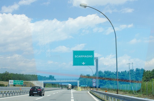
Arduinos are made in Scarmagno, Italy, a small town near the Olivetti factories on the outskirts of Torino. All of the circuit board fabrication, board stuffing and distribution is handled out of that small town. I was really excited to see the factories, and I’d like to share some photos of them with you.

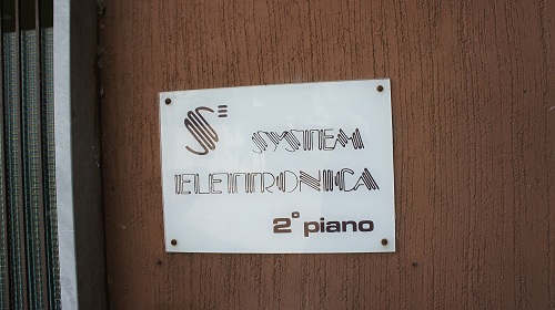
The highlight of my tour was “System Electronica”, the PCB factory which makes the Arduino PCBs.

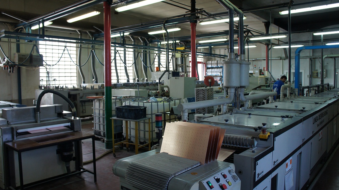
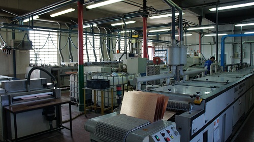
One charming aspect of System Electronica is the owner has the factory painted to match the colors of the Italian flag. In this wide view of the factory floor, you can see some of that in the red and white posts down the length of the facility.

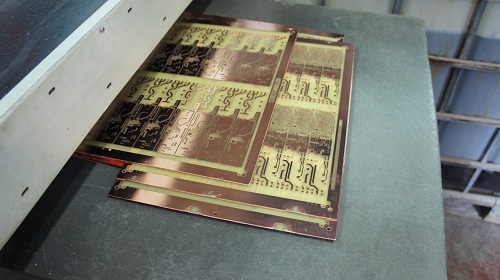
Arduinos start as huge sheets of virgin copper-on-FR4.

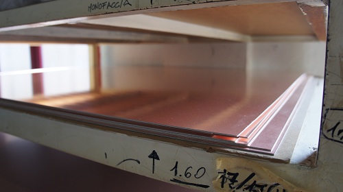
The sheets above are 1.6mm thick (the most common thickness for a PCB, which corresponds to 1/16th of an inch), and probably a meter on one side by about a meter and a half.

The first step in processing is to drill the holes: hole drilling is done even before patterning. This is because once the holes are drilled, you can use the holes to align the masks used to pattern the traces later on in the process. Hole drilling is also a dirty and messy process, which can damage circuit patterns.

Above is the CNC drilling head used to drill the boards. The blank copper sheets are actually stacked three-high so a single pass of the drill can produce three substrates.

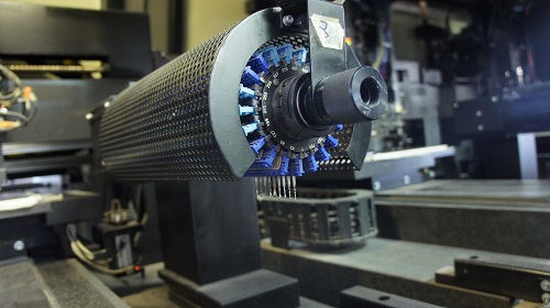
Above is the drill rack used by the CNC drilling machine. If you’ve ever had to muck around with creating NC-drill files, you’ll probably have seen the term “drill rack” used somewhere. This is what it looks like.

Above is the drill in action. It’s encoded in Ogg Theora; so, sorry if you’re using IE or Safari and you don’t have the codec installed. An HD version of the video is also available here. Flash is dead; long live HTML5! [note: I turned off video pre-loading to save bandwidth by just editing the attribute tags. That would have been a pain in Flash. Yet another benefit of HTML5!]

Every hole in the board is mechanically drilled, which is why via count is such an important parameter in calculating the cost of a PCB. This particular drill is a relatively small one. I’ve seen massive drill decks in China that slave four or six drill heads together in a truck-sized machine, processing dozens of panels at the same time; they drill so fast and hard that the ground shakes, even from several meters away, with every via drilled.

Above is a stack of finished, drilled boards that have been cleaned and deburred, ready for the next step in the process.

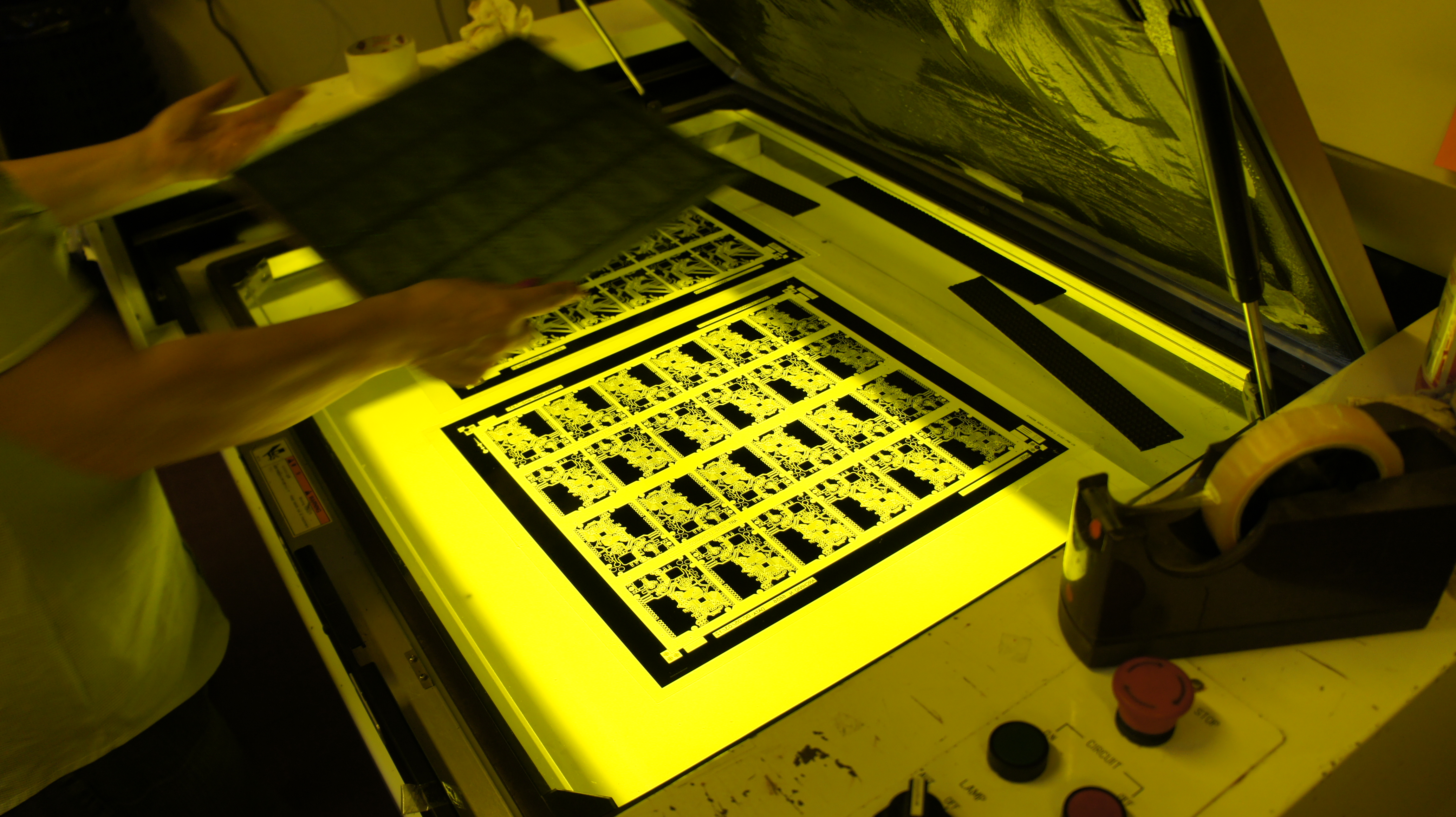
The next step is to apply a photoresist to the board and expose a pattern. At System Electronica, this is done using a light box and a high-contrast film. Other technologies I’ve seen include direct laser imaging, where the pattern is put on using a raster-scanning laser. Direct laser scanners are more common in quick-turn prototype houses, and film imaging is more common in mass production houses.

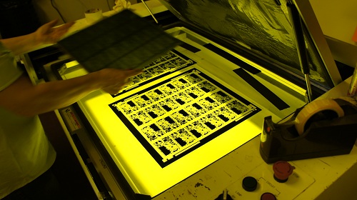
Above is a PCB blank being mounted into a light box for exposure. Note that most photos in this post can be clicked to reveal a much higher resolution version.

Above is what the board looks like before and after exposure.

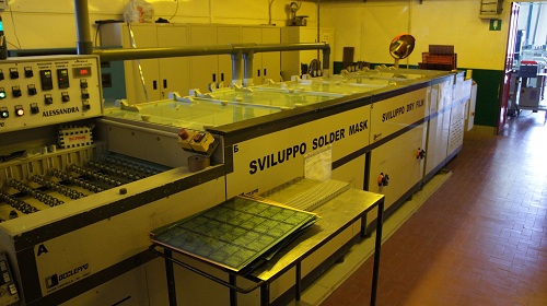
The boards are then sent into a machine to be developed. In this case, the same machine is capable of developing both the photoresist and the soldermask.

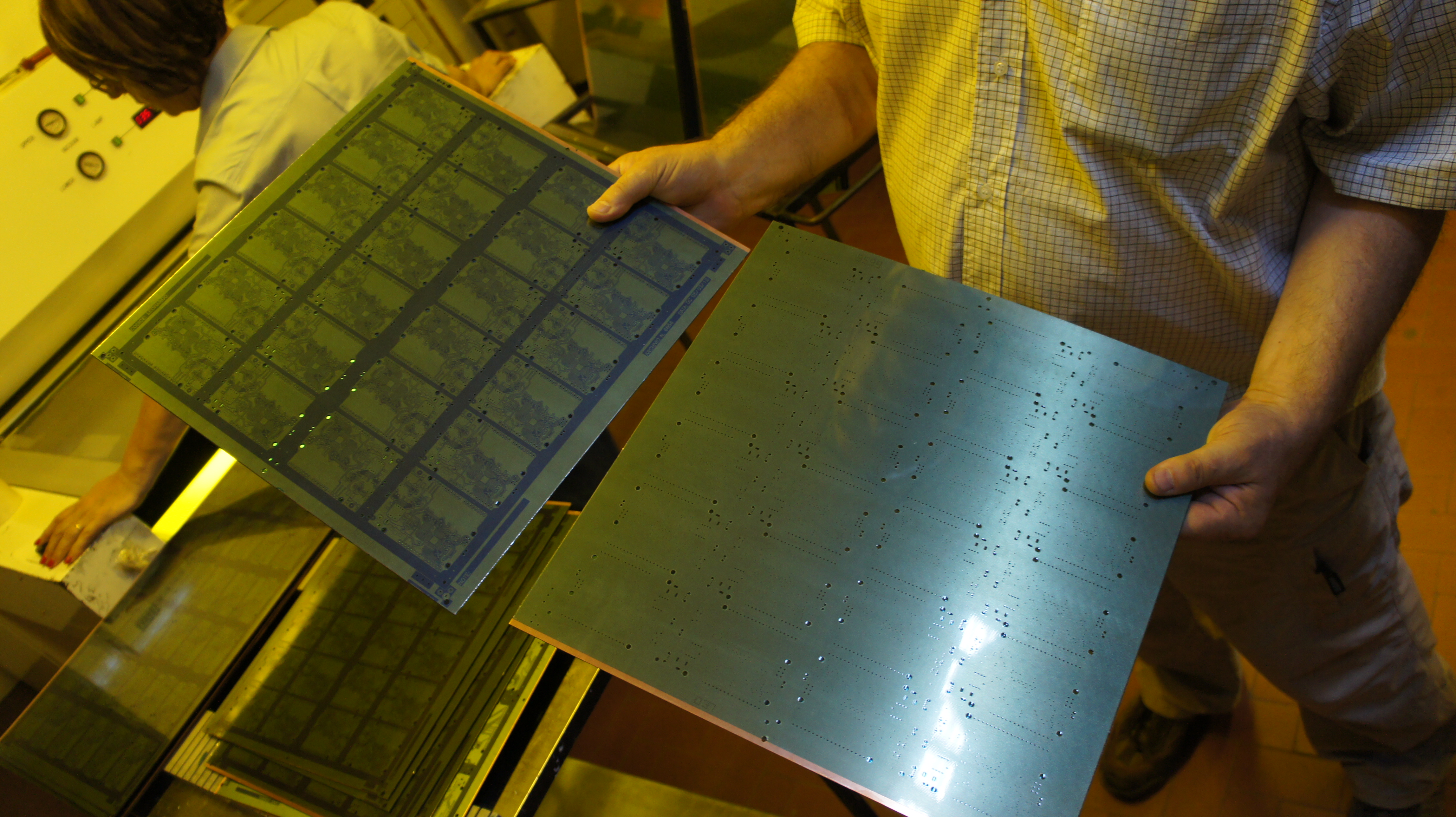
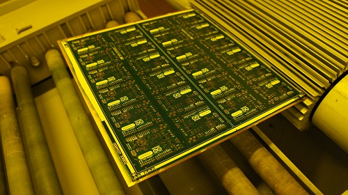
Above is an image of a developed board. It’s one of my favorite photos out of the factory. Also, there is just something cool sounding about “Codice: Leonardo”.

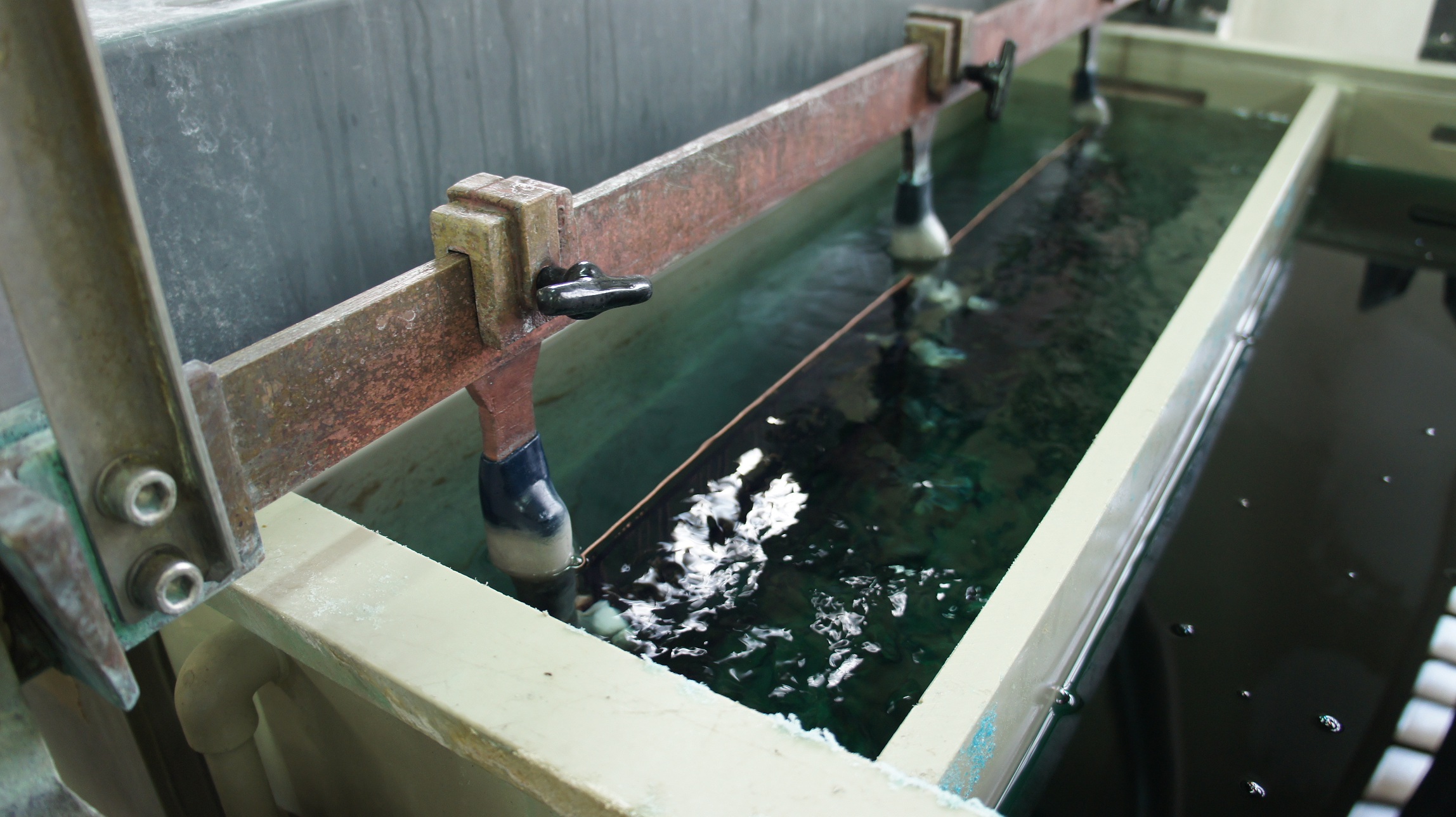
After photo-processing and development, the boards go through a series of chemical baths that etch and plate the copper.

The movement of the boards through the chemical baths is fully automated; this is necessary because between certain steps oxygen can spoil a board in a matter of seconds, so the transfer between the baths needs to be fast. Also, the baths contain caustic and harmful chemicals to humans, so it’s much safer for a robot to do this work.

[HD verison] As you can see, the boards swish gently back and forth in the baths as they are processed. Each bath has a different solution in it.

Once the boards are processed in this series of solutions, a dull, white plating (which I’m guessing is nickel) has developed on all the non-resist covered surfaces of the board, including the previously unplated vias and pads.

At this point the resist and unplated copper is stripped off, leaving just the raw FR-4 and the plated copper.

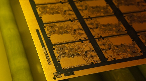
A final step of processing results in a bright copper finish. Note that the photo above isn’t of an Arduino board, as their boards weren’t going through the machine at the time when I was taking photos of it.

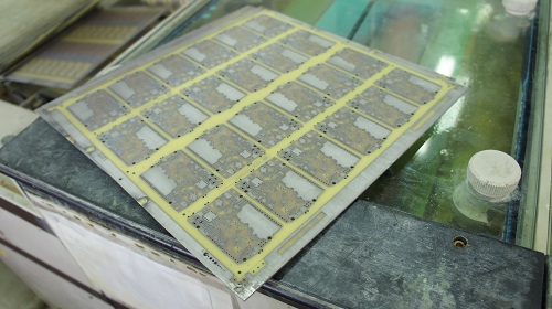
The boards are now ready to have soldermask and silkscreen applied. These are applied using a very similar process to the trace patterns, using a photomask and developer/stripper machine.

Above is photo showing a board with both soldermask and “silkscreen” developed. The silkscreen in this case is actually a second layer of soldermask. A very specific formulation of dry-film white soldermask was procured for team Arduino to create a sharp and good-looking layer that can resolve the intricate artwork found on Arduino boards. Other techniques I’ve seen for producing silkscreen layers include high resolution inkjet printing, which is better suited for quick-turn board houses, and of course the namesake squeegee-and-paint silkscreen process.

Once the boards have finished chemical processing, they receive a protective plating of solder through a hot-air solder leveling machine, and then move on to testing.

[HD version] Every board is 100% tested. This means that every trace has its continuity and resistance measured using a pair of flying probes. That’s a lot of probing, and the video above gives you an idea of how fast the probing is done. An alternative to flying head testing is to use clamshell testers, where a set of pogo pins are put into a fixture that can test the entire board with a single mechanical operation. However, clamshell fixtures are very labor-intensive to assemble and maintain, and require physical rewiring every time the gerbers are updated. So, in many cases flying probe testing can be cost-favorable and more flexible when compared to fixtured testing.

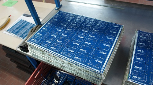
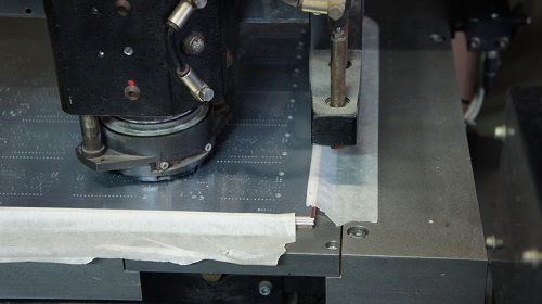
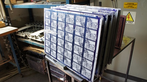
Above is a stack of near-finished PCB panels, ready for a final step of routing.

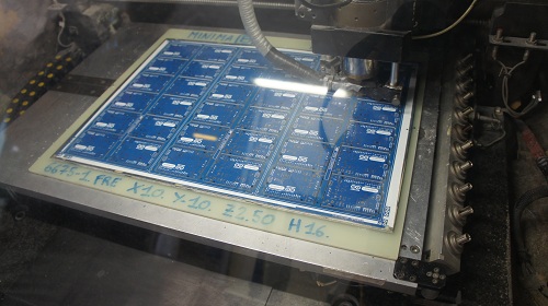
Before the boards can be shipped, the individual PCBs panels need to be routed so they can fit inside SMT machines. The boards are once again stacked up and batch-processed through a machine that uses a router bit to cut and release the board panels.

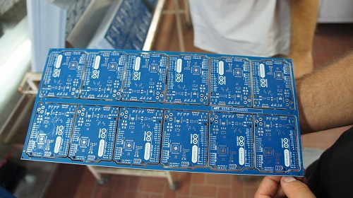
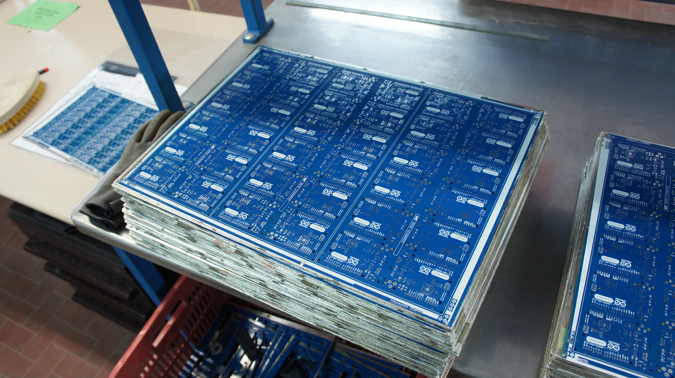
Finally, the boards are ready to ship on to the SMT facility. As you can see, the boards are panelized in a 2×6 format to make SMT processing more efficient.

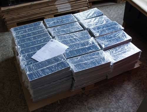
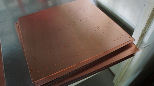
Here’s a veritable stack of about 25,000 bare Arduino PCBs ready to leave the PCB factory, moving on to be stuffed, shipped and sold to Makers the world around!

Many thanks to the Officine Arduino team and Davide Gomba in particular for taking time out of their busy schedules, showing me around, and patiently waiting as I expressed my inner shutterbug and general love for all things hardware…

MicroSD card FAQ

Friday, March 23rd, 2012

A while back I wrote an analysis of fake microSD cards. As a result of the post, I’ve received this question regularly via email:

“I’m trying to buy a thousand microSD cards for my embedded controller project. How do you qualify a microSD card?”

So, I thought it might be helpful to share my answer here.

There’s this awkward phase between the weekend project (where you buy your microSD card from Best Buy for $20 and have a no-questions return policy) and being Nokia (where you buy the same cards for $2 in quantities large enough to actually have leverage over vendors). When you source a few thousand cards at a time on the wholesale spot market, you’re basically on your own to control quality.

As far as process control, some vendors are easier to work with than others. Samsung will bump their part numbers based on die revs or other significant internal changes to the card. Sandisk, on the other hand, uses a very short part number for their cards, so you have no idea if the NAND on the inside is MLC or TLC, etc.; you just know the capacity and the card is simply guaranteed to perform to spec. To wit, Sandisk is very thorough about ensuring they meet the spec. However, it’s the edge cases that usually bite you in production; regardless of the spec, every die/controller combo has some character and your embedded controller may bring out some of that color. And, of course, there’s the fakes — Sandisk is a huge target for fakes, people who want to borrow their good name to sell you a batch of shoddy cards.

If you’re working with a distributor, get a copy of their authorization letter that certifies the relationship with the brand they are selling. It’s easy to fake the certificate, but it’s a good formality to pursue anyways. If you can, get the upstream brand to confirm the distribution relationship.

Aside from these supply-chain side things, here’s a check-list of technical tests to run on your cards:

For each new distributor:

1. I read out the CID and CSD registers and decode them. This is easy to do on linux with a directly connected microSD card. You cannot do this if the card is plugged into a USB adapter — you need to have the card plugged into a direct SD interface. The CID and CSD should look “right” i.e., the manufacturer ID should make sense (unfortunately the manufacture ID codes are all secret, but I can assure you it’s not supposed to be FF or 00), serial numbers should be some big number, date codes correct, etc.

2. Do a “full write” test at least once. i.e., create a random block of data that’s the putative size of the card, and dd it into the card. Then, do an md5sum of the contents of the card. This will identify loopback tricks that fake capacity. This is a relatively common trick that is surprisingly hard to detect, because many cards are only used to less than 50% capacity in real life.

3. Do a reboot test, to understand the behavior of the controller/die combo during ungraceful powerdown. It’s less important on systems that can never have their battery removed.

Before the test, I do a recursive find piped to md5sum to get a full map of all the files in the card. Then, I use a script that writes a random amount of /dev/urandom data in odd-sized blocks (ranging from a couple hundred bytes to a couple megabytes) to the card and then calls sync, in a constant loop after boot. For each block written, the md5sum is recorded. At boot time, all old blocks are checked for md5sum consistency and then deleted. The system under test is automatically power cycled by cutting the AC power about once very 2-3 minutes plus some random interval (depends on how long it takes your device to boot). I cut on the AC power side to capture the effects of the power decay curve of the wall adapter; the logic goes that a clean power down is less likely to cause problems than a gradual powerdown. I run the test on a cohort of at least 2 systems for 2 days straight. If you want to get fancy, you have the system upload its statistics to a server so you can see exactly when it starts to fail. After a couple of days, I extract the card from the system and redo the recursive find with md5sum to verify that no non-critical files have been corrupted that would be difficult to notice without the comprehensive check. Be sure, of course, to ignore files that naturally vary.

I still don’t have a straight answer on why some cards perform better under this test and others fail miserably. Ultimately, however, every card I’ve encountered eventually corrupts the filesystem after enough cycles, it’s just a matter of how long. I feel comfortable if I can reliably get to ten thousand ungraceful reboots-while-writing before failure. Note that supposedly eMMC has design features that harden cards against these problems, but I’ve never had the luxury of building such high volume systems that eMMC becomes an affordable option. Besides, I consider giving users the ability to remove the firmware card and reflash it with new code using a common USB adapter an important feature, at least in the systems I design. Mobile phone carriers would think differently.

Of course, once a vendor is qualified, they can still send you bad lots.

For each new lot I get, I take a few cards and burn them myself and check they boot the system before handing them over the factory. I also manually inspect the CID/CSD to ensure that the manufacturer’s IDs haven’t rotated and I inspect the laser markings to ensure that the lot number changes (it should — if it doesn’t then they are pulling something wonky on you). I also compare the circuit trace pattern on the back, visible through the reliefs in the solder resist coating. If you have easy access to an X-ray machine (some CMs have them on site) you can go so far as to compare the internal construction in the x-ray to see if the dies have been revved. If all these are the same you’re probably good to go on the new lot, but I do pay attention to the failure rate data in the first couple hours of production just to make sure there isn’t something to worry about.

There’s probably a bunch of other tests, techniques and good ideas that I should be aware of…look forward to reading the comments!

China: Crowdsourced Tax Enforcement

Thursday, March 22nd, 2012

Riddle me this: how does a government enforce tax collection in a cash-only society? Cash has the wonderful property of being anonymous, and therefore hard to track. As a result, cash businesses often under-report revenues, thereby dodging a portion of tax payments.

China is primarily a cash-driven economy; few local places will accept payment cards of any kind (event rent payments are made in cash — a big, fat stack of cash, as the largest bill in China has an equivalent value of about US$15). As such, China has a big challenge around collecting taxes.

A solution to the problem is to go with a tax pre-payment system. At the beginning of every month, every business is required to pay an estimated tax. Proof of tax payment is issued in the form of “fapiao” (发票). They look a bit like the one below:

This fapiao represents tax paid on 10元 (元 is like the $ symbol, and colloquially pronounced “kuai”), so the restaurant I got this from probably paid about 1-2 kuai for this fapiao. When you settle your bill in a restaurant, in addition to getting the itemized receipt, you are supposed to receive a stack of fapiao of equivalent face value.

At the end of the month, the restaurant claims a tax refund on any remaining fapiao. As a result, fapiao are basically as good as money to the restaurant; hence, the fapiao are printed on watermarked paper with anti-counterfeiting measures, and employ serial numbers you can validate by sending an SMS to a government hotline. Also, restaurants have a strong incentive to omit a few fapiao from your stack, or completely forgo giving you the fapiao (they love it when foreigners dine, because they don’t know about fapiao — they get big business and they get the tax refund on it!).

So, how does one enforce the distribution of fapiao to customers? China’s clever solution is to make every fapiao a lottery ticket. If you look at the above photo carefully, you’ll see two metallized patches on the fapiao. You can scratch these off, and underneath might reveal a prize! Of course, the one I have above is a losing ticket — it just says “thank you”, with a serial number; but the prize can be thousands of kuai.

And so, China has crowdsourced tax enforcement, by potentially rewarding citizens with a cash reward for asking for all of their tax pre-payment receipts, and using them up by scratching off the prize areas. The cost of this massive force multiplier is vanishingly small, as all they are offering is the chance to win; I have only ever seen one winning ticket in the past couple of years, and it was for about 2 kuai. Still, it is a nice cultural touch to the end of a big meal, everyone sitting in a circle, scratching their fapiao to see if they won a prize for playing the part of a Chinese tax enforcement agent.

Of course, with every new system, new problems come in. One is that the waitstaff might nick a couple of fapiao en route to the customer. So now, to get your fapiao you usually have to go in person to a special counter that manages its distribution. And, of course, the restaurant can offer a bribe in place of the fapiao. Just this past month when I was visiting Harbin, I went to collect my lottery tickets and the lady at the register glanced at my 80 kuai receipt and offered to pay me 4 kuai instead of giving me fapiao! I was a bit surprised at how brazen the offer was, but in retrospect, I clearly was not from around there, and thus unlikely to be an auditor.