Archive for the ‘chumby’ Category

Copycat Corolla?

Sunday, December 13th, 2009

I saw this last week in China, and (un)fortunately traffic was moving slowly enough that I could snap a decent shot of it.

While Toyota is a household brand name, BYD is not — yet. For the uninitiated, BYD is a Chinese government-backed company that got its start making batteries for cell phones, and has expanded into just about everything, including cars (its strong background in making lithium ion batteries gives it a key part of the hybrid-electric car supply chain). Warren Buffet recently invested a couple hundred million dollars into the company, and everyone is expecting it to be a formidable player in the car market in the coming decades.

So when I saw this, I wasn’t sure if it was a stock Corolla to which a local enthusiast attached a BYD badge, or if it was a BYD copycat of our familiar brand-name Toyota car. Or, by some bizarre twist, perhaps Toyota is now using BYD to OEM their cars in China through a legitimized business relationship. I don’t know which is true, but according to the rumors I heard from people who saw this photo, this is actually a copycat Toyota made using plans purchased on the black market that were stolen from Toyota. Allegedly, someone in China who studies the automobile industry has taken one of these apart and noted that the welds are done by hand. In the original design, the welds were intended to be done by machine. Since the hand-welds are less consistent and of lower quality than the robotic welds, the car no longer has adequate crash safety. There are also other deviations, such as the use of cheap plastic lenses for the headlights. But, I could see that making a copycat Corolla is probably an effective exercise for giving local engineers a crash-course in world-class car manufacture.

chumby One hardware docs

Wednesday, November 25th, 2009

For those of you interested in the chumby One, the schematics and gerbers are now posted on chumby’s wiki in the hardware section. Hopefully, over time some of the hacks we’ve done will be documented on the wiki. Or, you could contribute and document your hacks there as well…it is a public wiki after all!

I think a short reminder is due about the hardware license attached to the schematics and gerbers. The topic of Open Source licensing is certainly one that has spawned many Holy Wars, with True Believers on all sides. Many accuse me of not being a “true” open source person, an opinion for which they are entitled to. I have always had my own opinion about open source that in some places run contrary to the popular opinion; for example, I find the GPL to be a bit burdensome at times, and the weight that comes with GPL code some times prevents me from using it or linking against it; instead, I have to find code that uses a “lighter”, less-restrictive license. However, I do firmly believe that both the company and the community are well served by sharing schematics for devices, and quite often these get out there regardless of the intentions of the maker. Oh and — in case it wasn’t clear, this blog is my personal, independent expression, so my opinions and views don’t necessarily reflect those of chumby Industries.

So, the first question many people ask is, why not GPL or CC? Originally, I thought I could attach any of the common, popular F/OSS licenses to these documents, but actually, they don’t apply, because hardware is a different beast than software. CC can’t protect functional works, and GPL is not a good match with hardware. The most important issue is that in hardware, patents are de rigueur, whereas software works are typically copyrighted. Patents are actually a fairly good match to hardware and they don’t have the same ridiculous shelf life that a copyright may have. As defined, patents grant limited rights to inventors of a “useful process, machine, article of manufacture, or composition of matter, or any new and useful improvement thereof” — a hardware-oriented legal mechanism drafted in a time before software existed.

Thus, the most important provision of the chumby HDK license is that in exchange for chumby sharing our technology with you, it requires you, under certain conditions, to share your technology with chumby. Simply put, it protects all of us from, for example, someone taking the chumby design, adding a GPS, patenting that combination, and thereby potentially preventing anyone else (including chumby) from creating a chumby with a GPS in it. I think this is a very reasonable provision, because essentially it creates a pool of cross-licensed patents within the chumby ecosystem. This pool is important because if a troll comes along and decides to threaten the ecosystem by asserting their patent rights to chumby or chumby-derivative products, then the entire pool of created patents are available to fight the troll.

That being said, it’s not a perfect license, so there’s a note in there asking you to reach out to us in case you need something different. In particular, there is an exclusion in there that prevents people from manufacturing chumby devices (you can modify and extend them, but not make them from scratch) based on these plans. Personally, I don’t like that exclusion — I’d love it if some university or non-profit felt free to use these plans to make cheap linux computers for teaching and/or bridging the digital divide — but I’m reminded by many people, both from the Open Source community and from the corporate interests of chumby, that there is a lot more to making a chumby than just the schematics. There are other issues, such as trademark, media licenses (such as MP3, On2 VP6, etc.), and code licenses (Adobe Flash) that need to be properly addressed to create a chumby product, and we haven’t figured out a good way to deal with all of the potential scenarios in a uniform fashion. So for now, it’s basically a friendly request to “contact us” and we’ll figure it out together.

And, now that I’ve made you suffer through reading that, the answer to the question that’s burning on the minds of almost one hundred submitters to the via-guessing contest:

The number of vias on that particular revision of the circuit board is 785 total. There are 298 8-mil vias, 350 10-mil vias, 8 12-mil vias, 14 13-mil vias, and 115 15-mil vias. A mil is 1/1000th of an inch, or 25.4 microns. The 8-mil vias are used selectively underneath the i.MX233 CPU, and I try to use them sparingly because they are the most difficult to manufacture (each via is individually drilled by a mechanical drill, one at a time, with a very tiny drill bit — the car-sized machine that does this is quite impressive, the whole floor trembles as it runs). The 350 10-mil vias are used elsewhere on the board for general signal routing. The 8 and 14 via counts are vias that are part of package layouts, such as QFN’s, that recommend specially-sized vias according to the manufacturer’s datasheets. And the 115 15-mil vias are primarily used to create the ring of vias around the PCB that form an EMI shield so that we can pass FCC without requiring an expensive metal shield over the PCB.

Some of you asked what a via is, and basically, it’s a vertical plug of metal that allows signals from one layer of a PCB to connect to signals of a another layer of a PCB. Below is a 3-D rendering of the chumby One PCB, cut-away, to reveal one layer of traces and the vias connected to it (click on the image for a larger version).

The region you are looking at is the back side of the CPU/memory region of the PCB, and the top-layer metal traces connected to them, as well as the vias that extend through the board. Five other metal layers are hidden from this view to emphasize the via locations.

The image above is generated by my PCB design tool, Altium Designer. Among other things, the tool unifies schematic, 2-D layout, and 3-D mechanical views in a single framework. It’s not a cheap piece of software, but in the context of a commercial project like this it easily pays for itself through the mistakes you avoid using the powerful analysis and visualization tools bundled into the package. Actually, in the spectrum of CAD tools, it’s quite reasonably priced; the really expensive tools are used for chip design, with licenses for a complete design kit costing upwards of $1 million/year (and trust me, for the price you’re paying, the software quality is utter crap). However, for people who are used to getting all their software for free, or at the price of a couple hundred bucks maximum, the idea of paying even a couple thousand dollars for a tool seems expensive, until you balance that off against the cost of a prototype run and a last-minute ticket to China to fix a mistake you didn’t catch at design time because you couldn’t visualize the problem adequately.

Below is an animation I had previously posted of a real PCB, as viewed in an X-ray machine. You can see the bobbin-shaped vias in the animation as the board rocks back and forth.

I wasn’t actually thinking anyone would try to count all the visible vias — kudos to those who put in that effort (omg follower I can’t believe you did that!) — but there are also many vias obscured by components on both sides of the PCB. I wanted to make sure there was some element of luck and chance involved, to give a bit of a disadvantage to people who happened to have access to AOI systems that can automatically count the number of vias using image-recognition algorithms.

The median guess was 463 vias, and the average guess was 495 vias. The closest guess was by “Clever_Screen_Name” at 781 vias (who, ironically, asked what a via was…just a lucky guess? or being ironic?), just an error of 4 vias from the actual count of 785. Congrats, email me to claim your chumby One!

Thanks to everyone else for playing the game — quite an overwhelming response, it took me a while to go through all the comments and tally the guesses. For those who didn’t win, you can still buy one at the chumby store. Remember, the launch promotion is ending soon, and the price will go up to $119 from $99.

Happy hacking!

chumby One

Friday, November 13th, 2009

The chumby One is finally released. You can buy it now for a $99 “chumby insider” pre-order price; once we start shipping, the price will go up to $119.


While I’ve been working on several new hardware platforms for chumby, this is the first of the crop to hit the market. This one made it out before the Christmas season because it is an evolution of the original chumby design, now called the “chumby classic”, as opposed to a completely new form factor for the device.

The key goal of the chumby One platform was cost reduction: my first sketches for the device were drawn on the back of a napkin about a year ago, back when the stock market was in a free-fall and losing several hundred points a day. Unfortunately, the chumby classic hit full-stride launch in the middle of the worst economic downturn since the Great Depression, and its cute cuddly form factor comes at a fair bit of a price tag that many couldn’t stomach. So, I did what any entrepreneur would do in a recession, I suppose … scale back, and take a good hard look at everything and try to build a product that is cheaper, faster, and better for the market, to try and win new customers, and to retain the loyalties of our existing customer base.

Fortunately, around that time, a Freescale apps engineer contacted me about a new CPU (the i.MX233) they were going to launch in 2009 that could hit a remarkably low price point. So, I drew up some strawman renderings and did some cost scenarios, and in CES 2009, we circulated the idea around with a few potential customers to get feedback on the features and pricing. The idea sort of slow-rolled through the first few months of 2009, and after chinese new years, I taped out the first prototype board in late March. Around May we contracted an industrial designer to do some sketches, and by June we had a near-final ID; our first 3D printed prototypes were made around then (we couldn’t afford a mechanical engineering contractor I had to learn Solidworks and do the mechanical integration for the 3D prototype myself — since I enjoy learning new things, this was quite a rewarding experience). In July, we inked a PO for steel tooling and by August we had first-shot plastics. September was spent refining and debugging the design, and October was spent doing more testing, refining, and ramping up mass production. And, here we are now, in November. When I wrote this, the first shipment of chumby Ones were somewhere 35,000 feet above the Pacific Ocean en route to LAX. As for the i.MX233, I believe we are one of the first devices on the market to use it…I even got a quote in their launch press release last August, although I couldn’t refer to the chumby One by name at that time.

Just to give you an idea of what the final assembly line for the chumby One looks like, below is a video of a part of the assembly line:


[flashvideo file=http://www.bunniestudios.com/blog/images/c1mp_line.flv /]

In addition to being about half the price of the original chumby, the new device added some features: it has an FM radio, and it has support for a rechargeable lithium ion battery (although it’s not included with the device, you have to buy one and install it yourself). There’s also a knob so you can easily/quickly adjust the volume. But I don’t think those are really the significant new features. What really gets me excited about this one is that it’s much more hackable. The most significant improvement is that the firmware is stored on a microSD card.

The microSD card isn’t replaceable from the outside — this is to prevent non-hackers from pulling it out and wondering why the device isn’t booting anymore — but if you take the back panel off (screws this time, no glue seals), it’s fairly easy to access. The key here is that no longer do you have to worry about bricking your chumby device: if you screw up the firmware, you just pull it out, mount it on your dev box, and dd a new image onto it. Also, microSD is a “managed” NAND device, unlike our previous generation device which used a raw NAND device. This means that we don’t have to rely on a MTD layer for the filesystem, and instead we can directly drop ext3 onto the device. While we still mount the root partition as read-only to harden the device against accidental damage, unlike our original cramfs implementation, you can trivially remount it as read/write and modify the linux on the device. Also, our OS image takes up only a small portion of the total device capacity, so there’s actually over a gigabyte of extra space on there for you to load extra applications and libraries.

Significantly, what’s good for the hackers is also good for the developers. Because of this additional flexibility, we could add a ton of great features into the OS. For example, the chumby one supports certain 3G modems, and will serve wifi as an access point through the 3G modem (it can also serve as an access point for an ethernet connection provided via a USB-to-ethernet dongle as well). This is really slick, because that makes it basically a 3G to wifi router; it is enormously useful when I’m traveling and I need to create a wifi hotspot for other devices to use. Of course, this feature isn’t exposed yet at the mainstream user level, but if it turns out to be a popular application it’s something we could wrap a GUI around and make it more friendly to use. There are also other little refinements, such as if you plug a USB keyboard into a chumby One, it will automatically pop up a console shell that you can type into; very handy for times when you can’t ssh in, like when you are debugging network scripts. It also has high-speed USB2.0 support, so unlike our previous generation device, you can plug a USB camera into this one and grab images at a decent speed. And yes, we’ve booted Android on the chumby One. Android runs on linux after all, so why not? Eventually we’ll get these hacks documented on the chumby wiki (heck, maybe even compile them into a book), but right now we’re a little pre-occupied with making sure the product launch goes smoothly. Actually, to give credit where it’s due, most of these cool hacks were implemented by xobs (remember him? he ported quake on the chumby classic), not me — I’m just the hardware guy, xobs is the software guru.

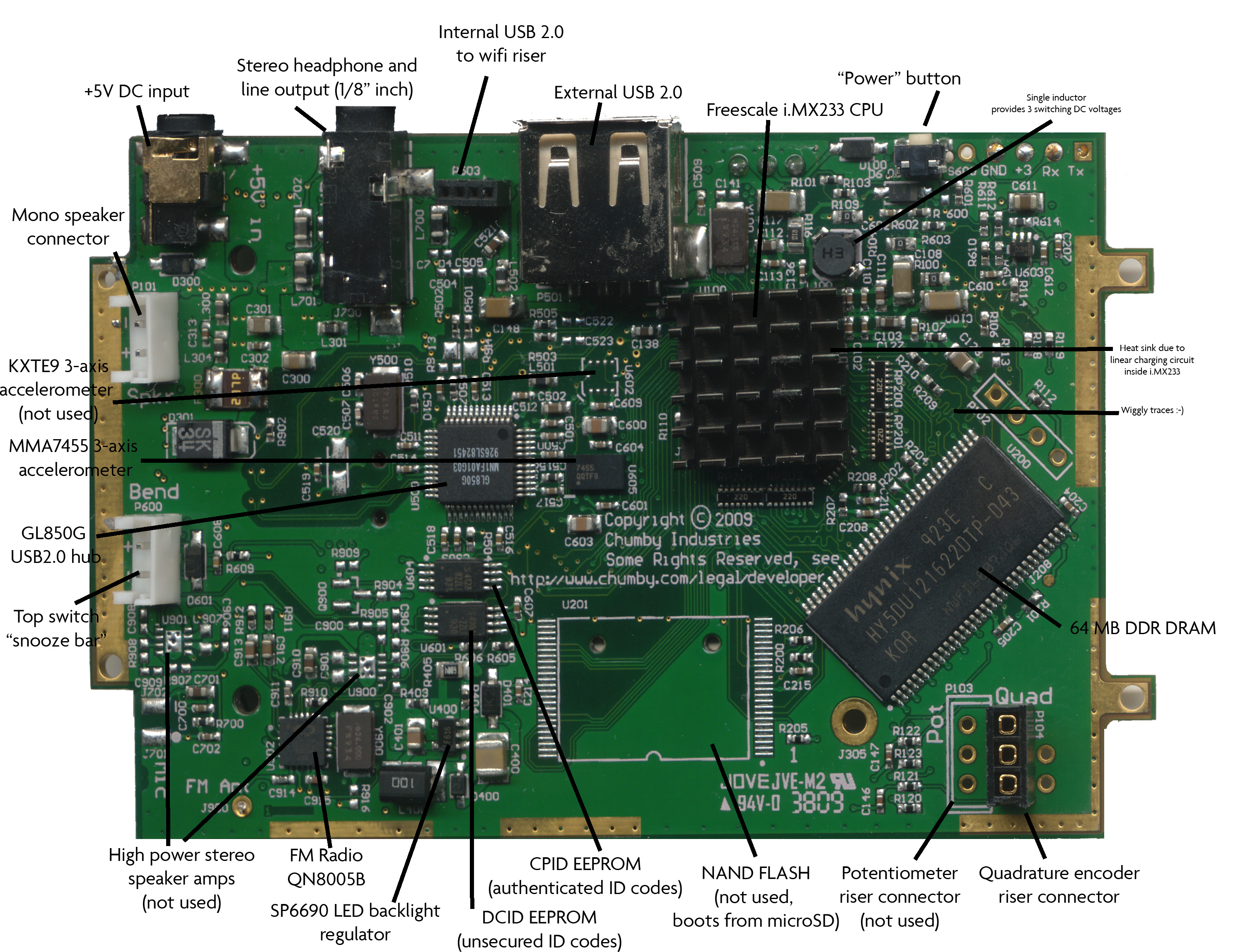
Below are some annotated photos of the chumby One mainboard. Schematics and gerbers are forthcoming, should be up in about a week or two; the GPL source code is already up.

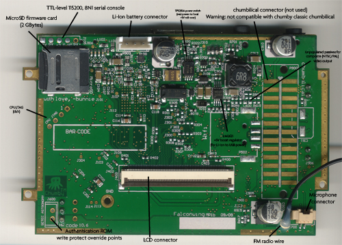
This is actually a pre-production pilot board. The mass production board is basically identical to this, with some minor tweaks to enhance compatibility with the SMT machines we use in China. There’s a couple of noteworthy points about the board. First, the footprints are available on the board for you to populate some parts to break out a composite video signal (NTSC or PAL). We’ve actually wired this up and confirmed that it works, and it’s pretty neat for presentations where you want to plug into a projector and show a crowd of people some widgets. There’s also a pair of test points on the board labeled “SETEC ASTRONOMY” that you can use to bypass the write protect on our authentication ROM, in case you want to wipe out the keys we use to authenticate your chumby. I can’t think of a real reason why you’d want to do that, but I added them on the principle that hardware you own shouldn’t hold secrets from you, so if you don’t like it you can nuke the encrypted access codes we put into each device (of course, it means you no longer have the codes to fetch widgets from our servers, but hey, it’s your hardware, void the warranty and do what you want with it). The security system is actually a bit convoluted on this device, but it uses basically the same, published protocol we employed on the chumby classic with some enhancements to leverage the internal AES engine on the i.MX233 to save the cost of an external cryptoprocessor unit.

One other really cool thing about the motherboard that I’d like to point out is that the power regulators are embedded inside the CPU. And they aren’t just linear regulators, they are switching regulators. And they just aren’t any switching regulators — this switching regulator derives three voltages using just a single inductor. How cool is that? Mad props to the guy who designed that system. The insanely high level of analog integration on this CPU — it pulls in the audio codec, power regulators, speaker amplifier, USB PHY, video DAC, battery charger and more — is one of the key things that has allowed me to create a system that you can buy at an affordable price.

If you’ve seen any of the chumby classic boards, you’ll instantly recognize that there are also mounting holes and features so this board can be retrofitted back into a chumby classic. That’s very intentional, although chumby doesn’t currently have a schedule to put this into a chumby classic; the classic line costs a lot to produce for more reasons than the PCB (think hand-stitched Italian leather). There’s also a couple of technical issues with integration, the most significant being the brutal thermal environment inside the chumby classic: the CPU contains the battery charging circuitry, and unlike the main supply, the charger circuit is a linear regulator so when charging it puts out a lot of heat. This is why we added a heatsink to the CPU, so we could charge the battery at maximum rate without having to throttle the CPU’s activity. I’m not quite sure how I would solve this problem if I were to put the board into a chumby classic, since there are no cooling holes in the device. I also get the sense that there wouldn’t be very much interest in a chumby classic that was a little bit cheaper, but still lacking the much-requested rechargeable battery: I am stuck between a rock and a hard place. However, the initial reactions to the battery in the chumby One are an interesting study in consumer psychology. For some reason, even though the chumby One is smaller and lighter than the chumby classic, and does largely exactly the same things, people don’t feel like it should have a rechargeable battery; they have no intrinsic desire to pick up the chumby One and carry it around. Just goes to show how much form influences a consumer’s perception of function. Also, as a very important note to intrepid hackers who want to try to retrofit one of these boards into their chumby classic: even though the footprint is identical, the chumbilical is absolutely not compatible with the chumby classic. For one thing, the chumby classic gets 12V from the chumbilical, and this device expects 5V. So if you were to just solder on a header and plug it into a chumby classic housing, you would get quite a cloud of smoke out of the device!

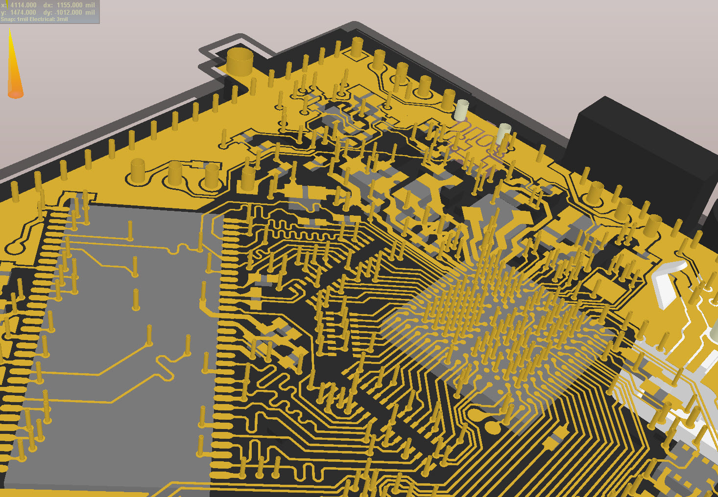
Also, as a little game for the readers, I will award a chumby One as a prize to the first person who can most accurately guess the number of vias on the chumby One circuit board based on the photos in this post. It’s a bit like one of those competitions where if you can guess the number of jellybeans in a jar you get the jar of jellybeans. This is vias not counting through-hole pads. Since the gerbers aren’t posted yet, you can’t cheat and use a CAD program to count the number of vias. :-) I’ll end the contest once the gerbers are posted, in about a week or so.

Nokia Schematics!

Sunday, July 26th, 2009

I was wandering around on a rainy Saturday afternoon in the mobile phone market in Shenzhen and I spied a stall keeper working on a phone motherboard. Unlike most of the other folks in the market, he was working from a set of schematics — that got my attention. I asked him where he got his schematics from and he kindly dispatched his young son to walk me over to the small tool shop on the other side of the market where, buried underneath a pile of single-use BGA SMT stencils, was a collection of mobile phone schematics for just about every phone made.

I don’t know about you, but getting my hands on schematics gets me really excited. This is like, the Ultimate Hardware Geek Pr0n. Sure, undressing a mobile phone and revealing its tender innards to my gaze — the sweet perfume of flux residue unleashed, curling into my nostrils — is one level of hardware voyeurism. But, getting the schematics for the phone and peering into its very circuit diagrams — that’s a whole new level, like tearing off the undergarments and ravaging the bosom of the phone. I was excited. I brought the manuals to the clerk and asked how much…wincing at the price I may have to pay to bring these prized morsels back to my hotel room. I breathed a sigh of relief when he asked for only 75 quai — a little over $10 US — for the whole three-book collection. I didn’t even haggle. I grabbed my booty and ran for the nearest taxi.

Alright. Don’t take my double entendre too literally; it’s just fun to write that way. Anyways, on to the manuals…

As you can see, these are sold as service manuals.

A sample index entry.

Each phone has a scan of the circuit board that is annotated to call out the position and function of all the components. This helps with the repair process.

A detail of the schematic for the Nokia N95’s RF section.

The same publisher of these schematics also offers a wide library of schematics, including those for Samsung, Sony Ericsson, Motorola, and Chinese-local “copycat” phones (like the iPhone clone in the lower left hand corner).

It’s hard to say if these manuals are legitimate (in the sense that Nokia deliberately released the schematics for use as a repair guide), or if they were stolen and republished as a “repair guide”. I doubt, however, that they were reverse-engineered out of the phone, because the schematics contain references to codenames and lingo that would not be embedded directly in the circuitboard. A bit of searching around on Google reveals that these manuals are available for downloads in bits and pieces on various websites, but they all seem to derive from a Chinese origin, and not from Nokia directly.

When I give talks about Open Hardware, I emphasize that it’s fundamentally impossible to keep hardware closed, because the source is the same as the product. Schematics can be derived out of a circuit board layout — a completely legitimate activity under US law. There are shops in China that will pull out a netlist in a couple days for under $1k, and services in the US that will take a bit longer and cost you a lot more. Significantly, there is a whole lot more that goes into building hardware than a mere schematic design: it takes me days to capture a schematic, but it takes me months to get it into mass production. Thus, I believe that publishing a schematic makes the product more serviceable and more useful, yet has little negative effect on your competitiveness in the marketplace. This is a key difference between software and hardware, as the time between writing software and publishing it to “production” can be as short as a few seconds for web-based services.

From my personal perspective, having the schematics is handy for a number of purposes. Aside from satisfying a general curiosity about the phone’s structure, it’s interesting to see the details on how certain sub-circuits are implemented. For example, when I learned electronics at MIT, they never directly taught me how to do EMI mitigation, or ESD protection. While I know the theory behind it, the implementation is trade-craft know how; these are subjects where experience trumps knowledge. Therefore, seeing Nokia’s take on it expands my understanding of the subject.

The schematics are also very useful because of Nokia’s buying power. Picking the cheapest part for a mass-produced hardware design is a tricky exercise; when you leave the realm of buying a few hundred or thousand pieces at a time and move into really high volumes, often times the price of the part has less to do with its design features and more to do with its physical dimensions and who is buying a lot of it. If someone like Nokia is buying millions of a certain part a year, the supply of this part is very stable, lead times are shorter (usually), and the price goes down. So, if you’re a small company and you want to build something cheap, you want to pick parts out of the Nokia supply chain because you indirectly enjoy the benefits of Nokia’s buying power. Thus, these schematics are a good starting point for sourcing cheap parts for production.

Update: got the books for Sony-Ericsson, Motorola, and MediaTek-chipset phones. Found only one Samsung book and it was very out of date. From my observations, the books left on display in these small shops are remainders — typically a little older, perhaps a little less popular. I had to scour the market to find a few of the more recent books, which probably means they are out there but I just don’t know the right person yet. Interestingly, the MediaTek-chipset series of books included some “how-to” manuals on using the chipset to build your own phone. This may be part of the “open” repository of hardware knowledge I previously mentioned in my post about the Shanzhai phone-copiers-turned-innovators.

Neat Hack

Tuesday, April 7th, 2009

dieselkraft.net has a nice photo series illustrating how Ole added an 800×600 display to a chumby by fabbing an adapter PCB and dropping the whole assembly into a beautiful antique pictureframe. Now that’s seriously cool…and I love the dieselkraft domain name!