Archive for the ‘name that ware’ Category

Winner, Name that Ware July 2024

Friday, August 16th, 2024

The ware for July 2024 is an Ingenico Axium DX8000. I hadn’t had a chance to tear down a modern POS terminal myself, so it was pretty interesting to see all the anti-tamper traces built into the product (thank you jackw01 for sharing it!). I wonder how effective these are, and how they mitigate manufacturing variations to prevent false positives. It looks like they use some custom IC to drive the serpentine traces, so presumably the chips are smart enough to do a training phase that calibrates to the environment and they just look for a “delta” on key metrics to flag a problem. Every computer already has self-training drivers that respond to manufacturing variations (in the DDR busses and high speed comms cables such as HDMI, USB-C, Ethernet, etc.), so I imagine this is fairly solid technology.

Still can’t help but wonder if the terminals can be remote-DoS’d with a relatively simple device that radiates signals at the right frequency to activate the tamper triggers. Thankfully, I haven’t heard of such an exploit, yet.

Jacob Creedon had a strong first guess but Anon got the make and model almost exactly right, so I’ll give the prize to Anon. Congrats, email me for your prize!

Name that Ware, July 2024

Wednesday, July 31st, 2024

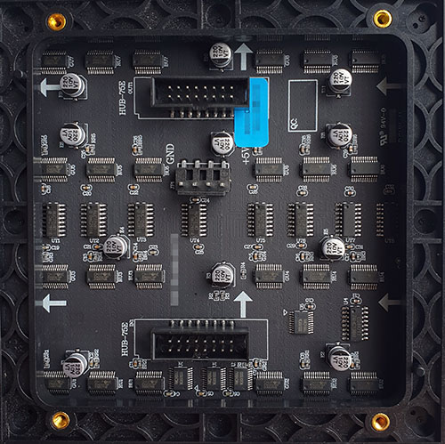
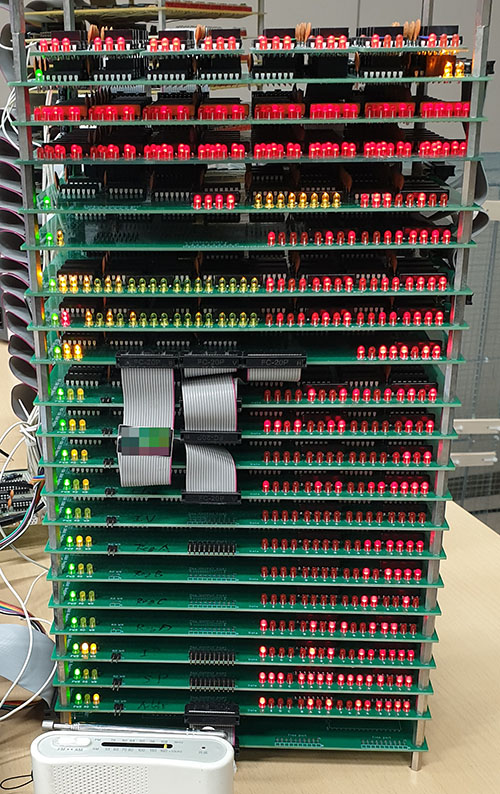
The Ware for July 2024 is shown below.

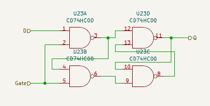
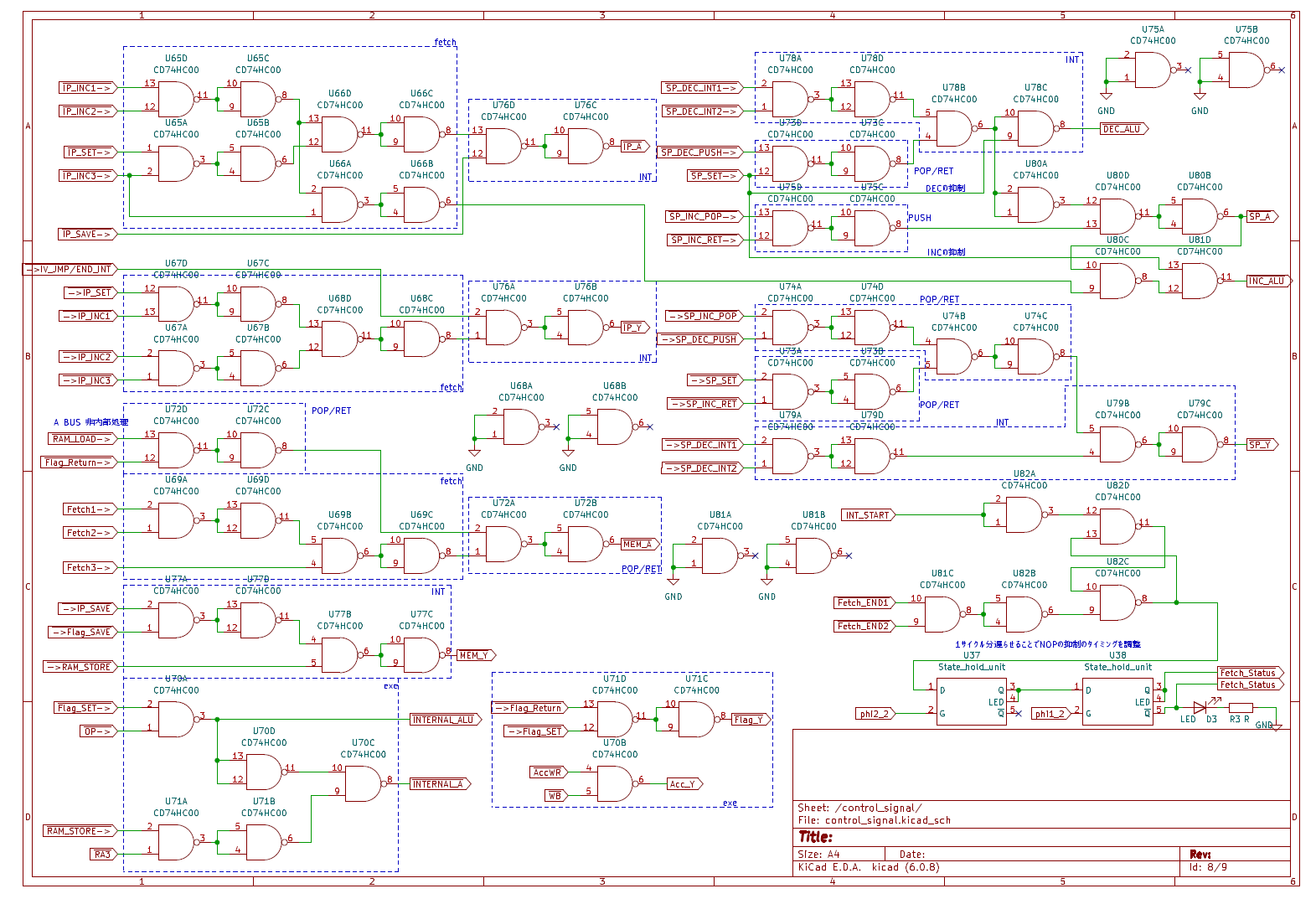
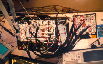
Thanks again to jackw01 for contributing this ware! The last two images might be killer clues that give away the ware, but they are also so cool I couldn’t not include them as part of the post.

Winner, Name that Ware June 2024

Wednesday, July 31st, 2024

The Ware for June 2024 is a hash board from an Antminer S19 generation bitcoin miner, with the top side heatsinks removed. I’ll give the prize to Alex, for the thoughtful details related in the comments. Congrats, email me for your prize!

I chose this portion of the miner to share for the ware because it clearly shows the “string of pearls” topology of the miner. Each chip’s ground is the VDD of the chip to the left. So, the large silvery bus on the left is ground, then the next rank is VDD, the next is VDD*2, VDD*3, and so forth, until you reach about 12 volts. The actual value of VDD itself is low – around 0.3V, if I recall correctly. Miners focus on efficiency, not performance, so the mining chips are operated at a lower core voltage to improve computational efficiency per joule of energy consumed, at the expense of having to throw more chips at the problem for the same computational throughput.

Along the bottom side of the image, you can see that the signals between chips cross the voltage domains without a level shifter. This is one of the things that I thought was kind of crazy, because there is a risk of latch-up whenever you feed voltages in that are above or below the power supply rails. However, because the core VDD is so low (0.3V), the ground difference between adjacent chips is small enough that the parasitic diode necessary to initiate the latch-up cascade isn’t triggered.

The whole arrangement relies on each chip maintaining its core voltage to under the latch-up threshold. But what controls that voltage? The answer is that it’s pretty much unregulated – if you were to say, run hashing on one chip but leave another chip idle, the core voltages will diverge rapidly, because the idle chip will have a higher impedance than the active chip but being wired in series, all the current of the active chip must flow through the idle chip, and thus the idle chip’s voltage rises until its idle leakage becomes big enough to feed the active chips in the chain.

Of course, the intention is that all the chips are simultaneously ramped up in terms of computational rate, so the energy consumption is equally distributed across the string and you don’t get any massive voltage shifts between ranks.

You’ll note the supplemental metal sheets soldered onto the power busses on the board. I had removed one of the sheets in the top right of the image. These bus bars are added to the board to reduce the V-I drop of the power distribution. Each string pushes 10’s of amps of current, so reducing the resistive losses of the copper traces by adding these bus bars in between chips measurably improves the efficiency of the hasher. If you look at a more zoomed-out version of the image, the distance between the chips actually increases as you go across the board. I’m not sure exactly why this is the case but I think it’s because one side is farther from the fans, and so they adjust the density of the chips to even out the air temperature as it makes its way across the board.

Anyways, at this massive current draw, any chip failure gets…”exciting”, to use a term of art. It turns out that a miner can operate with one busted chip in the chain. Since leakage goes up super-linearly with temperature and voltage, they basically rely on physics to turn the broken chip into a pass-through heating element. The voltage shift between ranks does go up slightly in that case, but apparently still by not enough to trigger latch-up.

That being said, latch-up is a big concern. Power cycling one of these beasts takes minutes — there is an interlock in the system that will wait a very long time with the power off to ensure that every capacitor in the chain has fully discharged. In order to prevent latch-up on a power-cycle, I imagine that every capacitor’s voltage has to be discharged to something quite a bit less than 0.3V. If you’ve ever poked around an “idle” board (powered off, but possibly with some live peripheral connector plugged in), you’ll know that even the tiniest leakages can easily develop 0.1V across a node, and 0.3V+ levels can persist for a very long time without explicit discharge clamps (I’ve seen some laptops designed with discrete FETs to discharge voltage rails internally so one can do a quick suspend/resume cycle without triggering latch-up). Since the design has no clamps to discharge the internal nodes (that I can see) I presume it just relies on the minutes of idle time on the reboot to ensure that the inherent leakage paths (which become exponentially less leaky as the voltages go down) discharge the massive amount of capacitance in the string of chips.

Of course, all these shenanigans are done in the name of efficiency and low cost. Providing a buck regulator per chip would be cost-prohibitive and less efficient; you can’t beat the string-of-pearls topology for efficiency (this is what all home LED lighting uses for a reason).

But, as a “regular” digital engineer who strives for everything to go to ground, and if ground isn’t ground you fix it so that the ground plane doesn’t move, it’s kind of mind blowing that you can get such a complicated circuit to work with no fixed ground between chips. The ground of each chip floats and finds its truth through the laws of physics and the vagaries of yield and computation-dependent energy usage patterns. It’s a really brilliant example that reinforces the notion that even though one may abstract ground to be a “global 0 voltage”, in reality, ground is always local and voltages only exist in relation to a locally measurable reference point – ground bounce is “just fine” so long as your entire ground bounces. If you told me the idea of stringing chips together VDD-to-GND without showing me an implementation, I would have vehemently asserted it’s not possible, and you’d have all sorts of field failures and yield problems. Yet, here we are: I am confronted with proof that my intuition is incorrect. Not only is it possible, you can do it at kilowatt-scales with hundreds of chips, tera-hashes of throughput, with countless deployments around the world. Hats off to the engineers who pulled this together! I have to imagine that on the way to getting this right, there had to be some lab somewhere that got filled with quite the puff of blue smoke, and the acrid smell that heralds new things to learn.

Name that Ware, June 2024

Sunday, June 30th, 2024

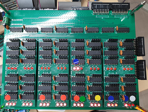
The Ware for June 2024 is shown below.

This one will probably be a super-easy guess for some folks, but the details of the design of this type of ware are interesting from an engineering standpoint. Some of the tricks used here are kind of mind blowing; on paper, I wouldn’t think it would work, yet clearly it does. I’ll go into it a bit more next month, when we name the winner. Or, if you’re already an expert in this type of ware and have circuit-level insights to share, be my guest!

Winner, Name that Ware May 2024

Sunday, June 30th, 2024

The Ware from May 2024 is a Generac RXSC100A3 100-amp automated load transfer switch. It senses when utility power fails and automatically throws a switch to backup power. Thanks to Curtis Galloway for contributing this ware; he has posted a nice write-up about his project using it. The total function of the ware was a bit difficult to guess because the actual load switch wasn’t shown – the relays don’t do the power switching; they merely control a much larger switch.

A lot of questions in the comments about why a 50/60Hz jumper. I think it’s because as a backup power switch, a deviation of the mains frequency by 10Hz is considered a failure, and thus, backup power should be engaged. I also think the unit does zero-crossing detection to minimize arcing during the switch-over. The system drives a pair of rather beefy solenoids, which can be seen to the left of the load switch in the image below.

And this is the inside of the 100-amp load switch itself:

For better images hit up Curtis’ blog!

I think Ben got pretty close in his analysis of the ware, noting the 50/60Hz jumper could be for mains failure detection. Congrats, email me for your prize!

An administrative note: my ISP upgraded the blog’s database server this past month. Because this blog was created before UTF-8 was widely adopted, the character sets got munged, which required me to muck around with raw SQL queries to fix things up. I think almost everything made it through, but if anyone notices some older posts that are messed up or missing, drop a comment here.

I’m also working on trying to configure a fail-over for my image content server (bunniefoo.com), which is still running on a very power-efficient Novena board of my own design from over a decade ago. It’s survived numerous HN hugs of death, but the capacitor electrodes are starting to literally oxidize away from a decade of operating in salty, humid tropical air. So, I think it might be time to prep a fail-safe backup server — a bit like the load switch above, but for bits not amps. However, I think I’m more in my element configuring a 100A load switch than an IP load balancer. The Internet has only gotten more hostile over the past decades, so I’m going to have some learning experiences in the next couple of months. If you see something drop out for more than a day or so, give me a shout!