Archive for the ‘Ponderings’ Category

Xbox360 RROD (Again)

Monday, January 21st, 2008

Nate just linked me to this post interviewing an inside source in Microsoft about the causes of the RROD. Now that I’m involved in hardware manufacturing of consumer devices, it’s a fascinating case study of what not to do, so I’m paying attention and taking notes.

A while back I posted that I was looking for an RROD Xbox360; I actually sent it off to MEFAS to get digested for solder joint inspection on the GPU through a process called “dye and pry”. In this process, the motherboard is flooded with red ink, and then the GPU is mechanically pried off the board. The red ink flows into any of the tiny cracks in the solder balls, and at least in theory, when you pry the GPU off the cracked regions will shear first so you will be left with visible red spots at the points of failure.

The findings were interesting. Below is what a normal ball looks like after the test:

(click on the image for a larger version)

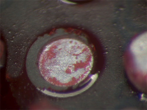
And here is one of several balls on the GPU that exhibited signs of partial failure:

There was also some “voiding” seen in the balls, e.g. trapped gas bubbles inside the solder balls that might serve as starting points for mechanical failure. Some voiding is expected, and there’s not a lot of data I can find correlating failure with voiding, but I could imagine in a stressful mechanical environment these things don’t help.
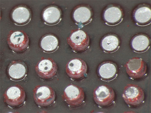
I was a bit puzzled by these results because you didn’t see any “catastrophic” failure — pools of red ink over a connection interface — just partial cracking. Partial cracking isn’t terribly uncommon, and many products work quite well despite such artifacts. However, after reading the article linked above, if Microsoft shorted safety margins around many of the design parameters to get the product out on time, it makes sense that the summation of many partial failures could lead to a total system failure — failures that have symptoms that vaguely cluster together but are difficult to point to any single root cause. Heisenbugs. Yuck.

Complex systems are a bitch to get right — and reliable. I think about that every time I step onto an airplane, or when I read about the space program. Respect to the engineers at Boeing and NASA!

CES08 Faves

Tuesday, January 8th, 2008

I saw a couple of things at CES this year that I actually thought were worthy of sharing. Usually it’s just faster, shinier, bigger, badder gadget after gadget — yawn. I’m pretty jaded, you could say, when it comes to gadgets. I still carry around and cherish my aging Blackberry, and despite the nasty inch-long crack in the front bezel everything works great. It’s almost a badge of honor–no iPhone could handle that kind of real-world abuse and keep on serving its owner so faithfully.

The most stunning thing I saw at CES this year was no gadget, however. It was a mock-up of the “motherglass” substrate that Sharp uses to make its 57″ LCD panels.

That is indeed the mother of all glass substrates.

There’s these huge frickin machines somewhere out there in this world that takes in that 9 foot piece of glass and deposits thin films of silicon on it, and images microscopic patterns into the films to make all those big, beautiful hi def LCD displays that the gadget freaks lust after. I lust after the machine that makes those panels–eight 57″ LCDs panels at a time. It makes those 12″ wafers at the Intel booth look well…small.

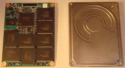
Other noteworthy things were the 128 gigabyte 2.5″ solid state flash drive for laptops that Toshiba had on display at their booth. I think there was another vendor that offered drives like this–Sasmung I think? But they didn’t have the circuit boards out for me to gawk at like Toshiba did.

Click on the image for a larger version of the circuit board. The drives are currently priced at $10/gigabyte, but hey, you know, Moore’s law will fix that eventually (although eventually is getting pushed out farther and farther as Moore’s law slows down). These drives are much faster than a standard hard drive for random seek, so it makes things like rebooting your laptop happen in half the time. Personally, I’d love to see this technology combined with a couple gigabytes of embedded DRAM and a smart caching chip to make one wicked fast mass storage device.

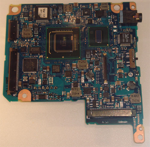
The other thing I saw that was neat is a Menlow-based motherboard, the first I had seen. I uhh…forgot what product it was in, it’s some Toshiba ultra mobile PC, but who cares about that; I’m sure engadget has some article on it if you’re into those kinds of things. The motherboard was the interesting part for me.


Click on the image for a larger version of the motherboard.

That’s it for now — I only got through about a third of the exhibits there so far, I had a lot of meetings for the past couple of days. If I find anything else really interesting tomorrow I’ll post it!

Battery Packs and Defects

Monday, January 7th, 2008

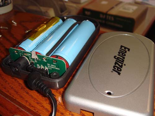
Recently, someone on the chumby forum noted that the Energizer ER-PHOTO battery pack works with the chumby. The ER-PHOTO is a handy little device that essentially emulates a 12V DC wallwart with a pass-through mode, so you can continue to use whatever is plugged into the battery pack while it charges. There’s a lot of devices out there that run off of 12V and use that classic 5.5mm DC barrel jack, so they are certainly handy to have around. As you can see in the photo below, the pack consists of 3x 1800mAh Li-Ion cells, which gives a nominal capacity of 20 Wh; of course, the step-up regulator is probably only 90% efficient or so, and the circuitry in the pack is fairly simple, so maybe it lacks the electronics to safely milk the last drop out of the batteries, resulting in a reduced delivered capacity.

Scott Janousek has a nice little writeup about how you can install the battery pack inside a chumby, although I’d be more than a little bit wary about doing what he’s written up–he’s taken the raw Lithium Ion cells out of their protective plastic housing. The electrical tape wrapping won’t provide adequate protection against puncture or impact (which is possible if you’re carrying around a chumby and you drop it). This can lead to cells catching fire in a way that can’t be put out easily (only class D fire extinguishers work on these fires, and many homes and small offices have only type ABC extinguishers).

I had a “near fire” experience once where my electric Braun shaver developed a loose connection to the rechargeable cell (it’s cold-welded on, and the continuous vibration of my luggage being dragged over cobblestones in Italy eventually wore the metal tab down) so that the charging circuitry saw a substantial series resistance in its path–my guess is it was trying to do current mode charging without paying attention to the voltage–and the shaver got extremely hot and started to carbonize the potting glue used around the components. I ripped the shaver apart and sprayed the battery down with freeze-spray to keep it from going into thermal runaway. I’ve also had a few Dell Latitude battery packs get scary-hot during charging–hot potato hot, where I had to juggle it from hand to hand while I ran it to the freezer to cool it down.

At any rate, I encountered a surprising defect in an Energizer battery pack the other day. One of the folks at the chumby office got one to evaluate, charged it, but it didn’t seem to work. So I took it apart, and lo and behold, the battery terminals weren’t soldered into the motherboard. Click on the photo for a larger version of the picture, to see the defect clearly.

I’m not quite sure how this got through QA–almost certainly there is a 100% unit test at the end of the line. Maybe the tabs made just enough contact for it to pass final test, and then vibration during shipping displaced them. It’s a very scary defect, however, as loose wires in battery packs can lead to hazardous conditions.

I can definitely see how a bug like this can happen in the process; I can just imagine two operators in China sitting next to each other, one of them stuffing the terminals and the other soldering them in, and then during shift change one of the stuffed but unsoldered devices gets mixed in with the soldered batch. Most factories put controls in place to try to avoid these kinds of process omissions–but mistakes do happen. To be clear, we all live in glass houses, as mistakes sometimes happen when building chumbys as well. Whenever I see a teardown of a chumby posted on the net, I take a keen look at the photos to see if all of the procedures were followed during the construction of the chumby device.

Winner of Name that Ware September 2007!

Saturday, November 3rd, 2007

Last month’s challenge was not necessarily to name a particular device, but rather to name the type of device that generates a class of audible interference. You can listen to the sound again if you need your memory jogged!

While many immediately recognized the sound as interference caused by a GSM or EDGE phone, Jered wins the prize for his very precise analysis of the root cause of the noise:

The reason for the buzz is the nature of time-division mulitple access (TDMA). In the US, we operate mobile phones at 850 Mhz and 1900 Mhz; in Europe, 900 Mhz and 1800 Mhz. Good so far; that’s not going to make noise that we can hear. TDMA fits more subscribers into the same bandwidth by assigning different terminals different timeslots (vs. CDMA, which uses black magic). These timeslots happen to be spaced 4.615 ms apart, yielding a signal envelope which looks a lot like a dirty 217 Hz square wave.

All sorts of things (like “wires”) are good at picking up a 217 Hz square wave at 0.5 W, and 217 Hz is conveniently smack dab in the middle of our auditory capabilities.

Congratulations Jered! Email me for your prize.

I thought this noise was noteworthy because a surprising number of people do not realize where it is coming from. I’ve often heard this noise on conference calls, and its fairly obvious that some participants don’t understand that their cell phone is causing this interference. The thing that befuddles most is the range at which this interference can occur: their phone could be well across the table, yet with the proper antenna orientation, the noise is loud and clear. Often times, the problem can be ameliorated simply by rotating the phone by about ninety degrees.

What disturbs me about this noise is that it’s a prominent reminder of exactly how powerful this RF transmitter is that I happily stick next to my cerebral cortex and my gonads on a daily basis. 0.5 watts is not a trivial amount of power! And of course, Bluetooth hands-free sets are not much better. Granted the power is lower, but Bluetooth operates at 2.5 GHz — and it’s no mistake that microwave ovens also run at that frequency, as it is absorbed particularly well by the water that makes up 60% of our mass.

While there is no conclusive evidence that cell phones cause any sort of biological harm, there is precedent for entire societies that have fallen victim to the myopic use of technology to better life. For example, even a child can tell you today that lead causes poisoning and brain damage…and so we remark at the Roman’s folly: “Gosh, what idiots! They sweetened their wine with lead and used lead pipe to deliver drinking water. Duh, of course the Roman empire collapsed.”

I often wonder if a millennium from now, people will read about us as we do about the Romans. “Gosh, what idiots. They stuck half a watt of radiation on their heads every day for decades at a time. No wonder they all died of debilitating brain disease.” Or, my other favorite is, “Gosh, what idiots! The made their clothes, cars, and even utensils out of plastics. Everyone knows that plastics outgas damaging free radicals. No wonder they all died of cancer”…and in the end, the meek did inherit the Earth.

Then again…there is no conclusive evidence that anything we do really causes that much damage. We’ve learned from the Romans and gotten more clever, and we use “model” organisms and sophisticated extrapolation mechanisms. But then again, those are just models, and there’s no such thing as accelerated lifetime testing on a real human being…and as any engineer knows who has done a lot of reliability testing, there’s always that one corner case that gets through (e.g., the Xbox360 Red Ring of Death). So with enough new technology entering our lives, the chance that we’ll encounter unforeseen consequences goes up and up. You and me — we’re the ultimate guinea pigs in this grand experiment with technology!

(Well Executed) Counterfeit Chips

Wednesday, October 17th, 2007

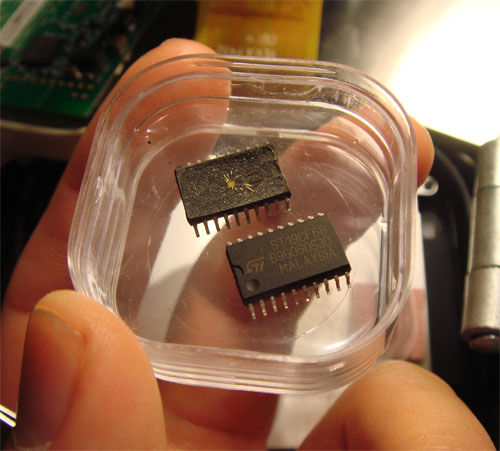
Below are two chip specimen, purchased from an Asian source, that were recently called to my attention. I borrowed them to write this blog post.

The chips claim to be ST19CF68’s, a “CMOS MCU Based Safeguard Smartcard I/O with Modular Arithmetic Processor”. It seems these chips are normally sold in smart-card or diced wafer format, but curiously, these are SOIC-20 packaged devices.

The top chip in the pair has its epoxy top dissolved, and this is what it contains:

Kind of a small die for such a complex MCU, especially in smartcard technology, where process geometries generally trail the mainstream by about 3 or 4 generations…and why are there 20 bondable pads on what should be an 8-pad part?

Zooming in a bit on the die, we find some interesting details:

Well, this chip isn’t made by ST…it’s made by Fairchild Semiconductor (FSC). No bueno.

And in fact, the die within is a Fairchild 74LCX244 “Low Voltage Buffer/Line Driver with 5V Tolerant Inputs and Outputs”, a much cheaper piece of silicon than the reputed ST19CF68 that the package was marked to contain.

Perhaps the most interesting thing about these specimen is the quality of the package and the markings:

Normally, remarked chips are pretty cheesy: they are sanded, painted over, or ground down before being marked, typically with just a silkscreen; rarely do you see a laser used to do the remarking.

These chips show no evidence of any kind of remarking per se. These are original markings — someone acquired blanks of the 74LCX244 chip, and programmed a production laser engraver to put a high-quality fake marking on an otherwise virgin package. I, too, would have been fooled by this up until the chip was decapsulated and examined under a microscope.

This leaves a lot of questions unanswered. How was someone able to acquire unmarked Fairchild silicon? Was it an insider, or was Fairchild sloppy and throwing away unmarked rejects without grinding them up or clipping off leads so they can’t be dumpster-dived and resold? The laser marking machine used isn’t one of the cheap desktop engravers either — the marks are done with a high-power raster engraver, and the engraving artwork is spot-on.

Then again, I shouldn’t be so surprised…I’ve seen brazen remarking of DIMMs in Saige market (Kingston seems to be a popular target for fakes), and many of the counterfeiters openly display their arsenal of professional-quality thermal transfer label printers and hologram stickers at their disposal.

If fakes of this quality become more common, this could present a problem for the supply chain. Clearly, whoever did this, can fake just about any chip they want, and they are gradually finding their way into the US market. Resellers, especially distributors that specialize in buying excess manufacturer inventory, implicitly trust the markings on a chip. I don’t think chip makers will go so far as to put anti-counterfeiting measures on chip markings, but this is definitely something that makes me wary.