The Ware for April 2010 is shown below. Click the image for a larger version.

I’m struggling to come up with meaningful commentary that won’t also give away the answer, so I’ll save the comments for when I provide the solution!
The Ware for April 2010 is shown below. Click the image for a larger version.
I’m struggling to come up with meaningful commentary that won’t also give away the answer, so I’ll save the comments for when I provide the solution!
The Ware for March 2010 was an N1100 Roku HD player. Matt Burkhard was the first person to correctly guess the model number, so congrats! Thanks for playing, and email me to claim your prize.
The chip with the epoxy around it is an HDMI PHY. I found it sort of amusing that the manufacturer went through the trouble of pouring epoxy over the pins of the chip…
Very tight on time this month, got delayed in Europe for a week due to Eyjafjallajökull and still digging myself out from under the backlog, so the commentary for this months judging and ware are a bit brief.
There’s an Easter Egg inside the chumby One (which is now on sale at Costco online for $99, cheaper than chumby.com’s $119 price!) that enables it to work with certain 3G USB modems and function as a 3G router (similar to a MiFi).
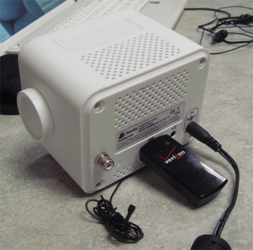
Above is a picture of a Verizon USB760 modem plugged into the USB port of a chumby One.
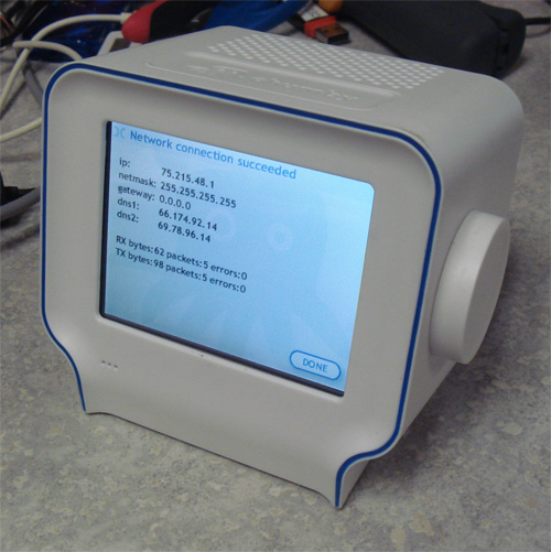
Use of the Easter Egg is documented on the chumby wiki, but it can be quite simple:
1. Plug in your 3G card.
2. Go to the Network Config screen by pressing the top button, going to Settings, then tapping on Network.
3. Select “create a new connection”, press OK, and wait for the scan to time out.
4. Select “Other”
5. Enter 3G as the name of the access point. It must have a capital G for it to work.
6. Wait for the subsequent scan to time out.
7. Select “Manual”.
8. Tap “OK” to select None as the encryption type.
9. Tap “OK” to select Automatic IP allocation.
10. Tap “OK” to confirm settings and connect to the network
To activate local wifi sharing, ssh into the device (or plug in a USB keyboard to activate the drop-down console) and use the command “touch /psp/start_ap” to flag the network setup scripts to configure your chumby One as an access point. Note that AP mode also works with other network sources, such as Ethernet-over-USB.
This works because the chumby One ships with a copy of pppd, hostapd and a set of glue scripts (courtesy of xobs) that allow it first to talk to the 3G network, and second to work as an access point that shares the 3G connection with other wifi devices using its internal wifi card.
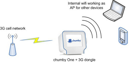
Since this is an Easter Egg, it has a few rough edges on it, such as no native UI to do things like configure your AP SSID and encryption mode, and for many GSM networks you’ll need to enter a custom username, password and phone number; but you certainly can ssh in and tweak the scripts to set those things up. Regardless, this is a very handy trick that I’ve used in hotels from Shenzhen to Tokyo to New York to set up a wifi hotspot (complete with Internet radio and chumby apps) on the road — the hack works with quite a few 3G dongles and networks (given a little tweaking).
I thought this was a great video; love what Kyle is doing at iFixit. I had heard about the e-waste farms in Africa but never seen footage of them, until now.
Something to think about.
usesthis.com recently posted an interview where I discuss what hardware and software tools I currently like to use to get my work done. This is a nice follow-on to a post I did about four years ago titled “The contents of my bag” where I summarized the things I carry around with me all the time. The only thing missing from the usesthis interview compared to my previous review is the bag that I use. Currently, it’s a Timbuk2 bag that’s been discontinued, but has the nice feature that it has both a shoulder strap and backpack-style straps with a muted charcoal-and-gray color scheme that is very versatile: it works for both more formal business meetings in Japan, as well as more mobile, casual situations such as hoofing it around the show floor at CES in Vegas. The bag has held up surprisingly well to abuse, although the left shoulder strap is starting to tear off and the tines on one of the snap-buckles for the main flap has broken, rendering it useless. This means my old Coach laptop bag is still the winner for durability, but unfortunately the single-strap design of the bag makes it tough to use when traveling.