For hackers, the fun part of consumer electronics is taking things apart and making them do things they weren’t originally meant to do. Since most consumer electronics devices are closed source, it’s a laborious process to do a hack; first you must reverse engineer the platform, and you are often relying on gut and instinct to grope around at the edges of your knowledge about the platform. Thus, on most platforms, it’s a challenge to reskin or case-mod the device, and deducing the location of a debug port and opening a console shell on the device is a big deal.
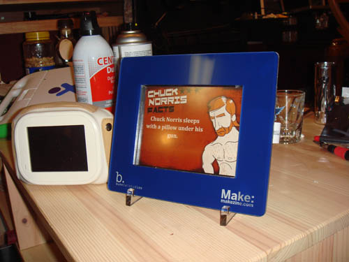
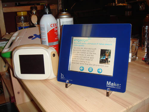
Chumby is different; it is open source, and designed to be hacked. For example, the serial port is spelled out on the silkscreen for you and there’s a backdoor to enable sshd, so it’s not big deal to bring up the console. Because of its hackability, you are enabled to do significant modifications due to the availability of all levels of design documentation—hardware, drivers, and application software. While it would be an enormous task to, for example, open up a Zune and put a larger screen on it, here, in this post, I will show you how to hack a chumby to have a larger, higher-resolution screen without too much effort. The native chumby screen is a 3.5” QVGA (320×240) display, but after you complete this hack, you will be treated to a 5.7” VGA (640×480) display.
Click on the photo for a larger version.
Selecting the LCD
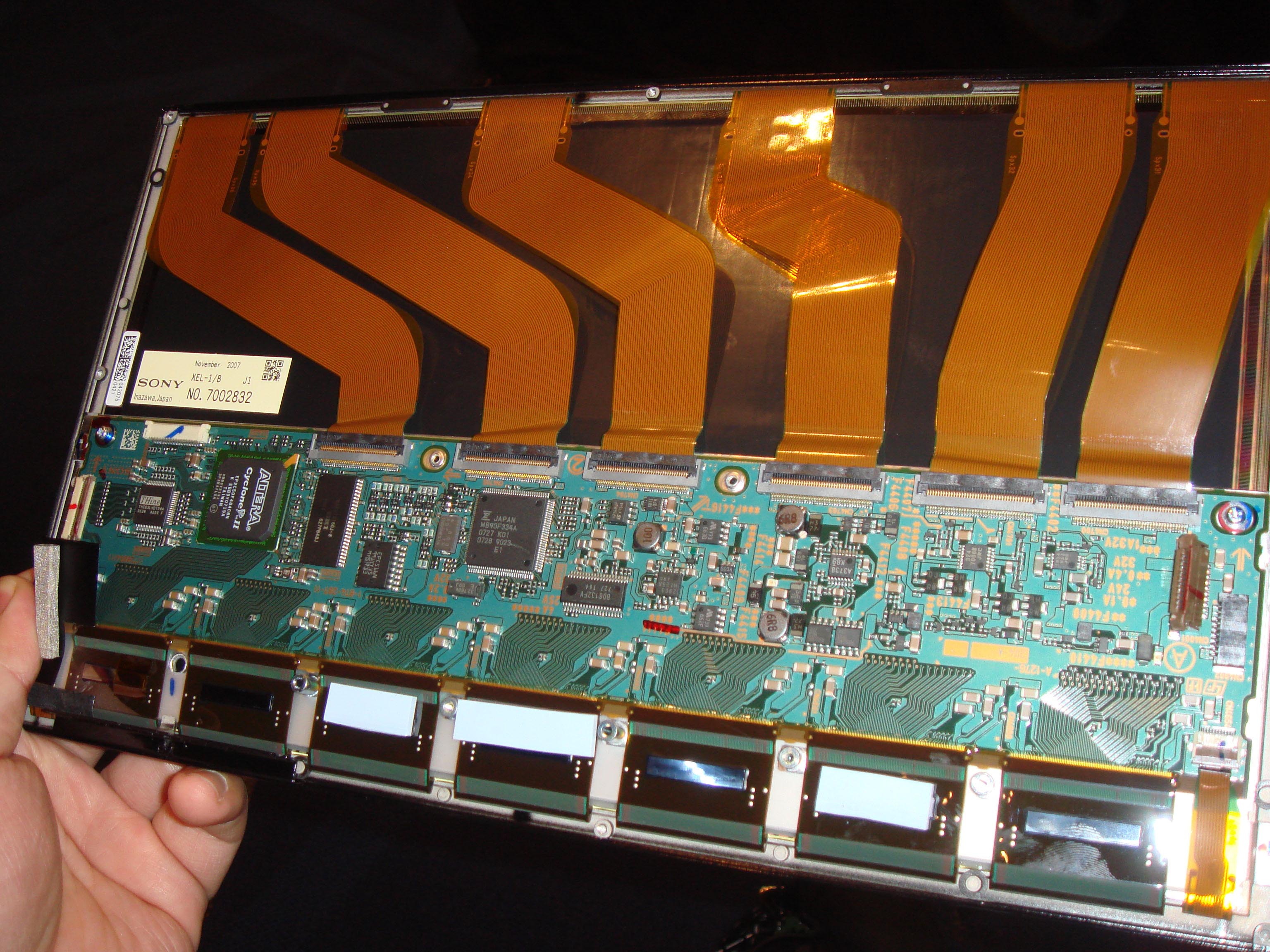
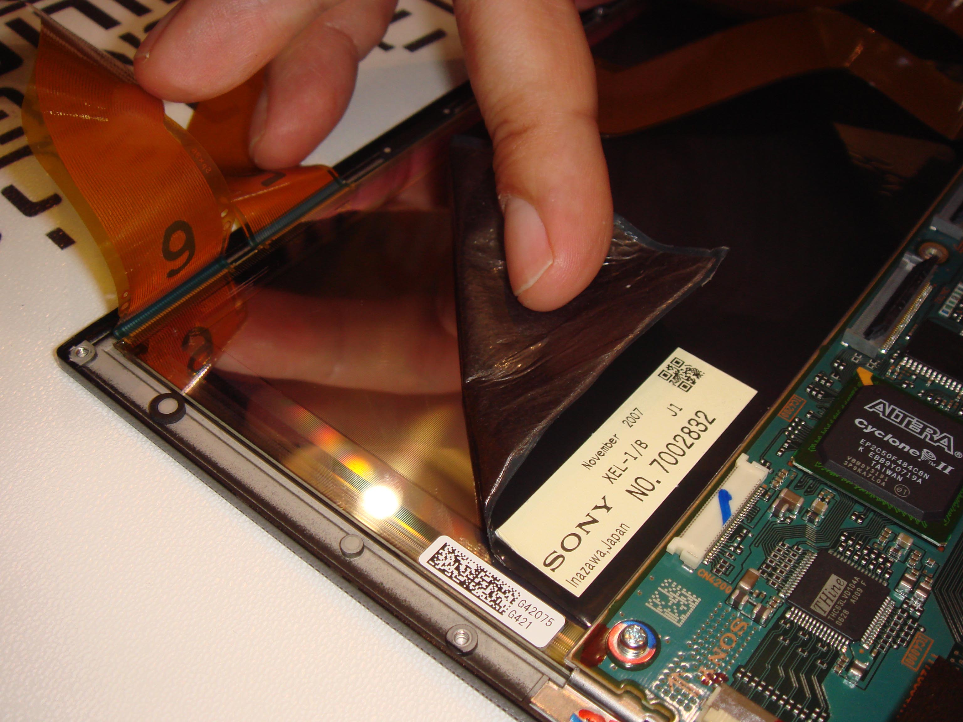
The first step in the hack is to select a compatible LCD that’s also conveniently available. For various reasons related to how the flat panel display market works, LCDs are difficult to purchase in their raw form. Fortunately, Mouser Electronics has a fair selection of LCD modules available and in-stock, although the price is no where near wholesale. I found that the Microtips MTF-TV57NP721-AV was a good match; you can buy these directly from Mouser for $150.80 by ordering part number 668-MTF-TV57NP721-AV. This LCD module uses a compatible signal format, has an LED backlight that works with a slightly modified chumby backlight driver, and also features a 4-wire resistive touchscreen, which is exactly the technology used by the stock chumby device. While the datasheet for this display is not available for convenient download, the datasheet itself is not marked proprietary or confidential, so I was able to secure a copy with a phone call to the local Microtips sales representative.
The Adapter Board
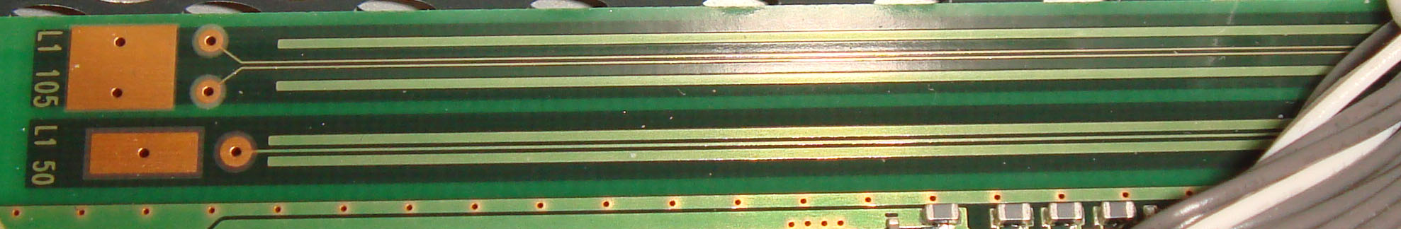
The next step is to build an adapter board between the chumby and the LCD. The adapter board is necessary because the flat-flex connector used by the Microtips LCD has a different size and pinout from the existing chumby LCD connector. The design of the board doesn’t require many components, as it is just rewiring the signals between two connector formats, but getting the design right does require attention to detail. It’s particularly important to make sure you get the location of the connectors right, so as to minimize the stress on the flex cables, and you need to be aware of the pinout inversion that happens between the two sides of a flex cable mating to the same type of connector: pin 1 goes to pin 50, and vice versa. Here is a link to the schematic for the adapter board, and a link to the gerbers.
 .
.
The bill of materials for the assembly is as follows:
Qty 	Digikey P/N			Description
1	RP20T5.6FCT-ND		5.6 ohm, 1/3W 1% 0805 resistor
1	RB070M-30CT-ND		Schottky diode, 30V 1.5A SOD-123
1	HFF-50U-02-ND		Flat flex cable, 50 position, 0.5mm 2”
1	HFF-36U-03-ND		Flat flex cable, 36 position, 0.5mm 3”
1	WM7077CT-ND		Molex connector, 0.5mm 50 position, R/A
2	487951-4-ND		4 position 1MM FPC top entry, R/A
1	929647-09-36-ND		36 position 0.1” header strip (breakaway)
6	A26242-ND		Shut headers with handle
1	100-4-18-BO-ND 		Flat flex cable, 4 position, 1mm, 1”
1	100R04-180BO-ND		7” version of above, use if above is out of stock…

Qty	Mouser P/N		Description
1	IL-FPR-33S-HF-N1	JAE connector, 0.5mm 33 position, R/A
1	668-MTF-TV57NP721-AV	5.7” VGA LCD panel with touchscreen

1	PCB per gerbers – can process through Protoexpress.com’s
         “No Touch” service for $72.45; less if you order in quantity
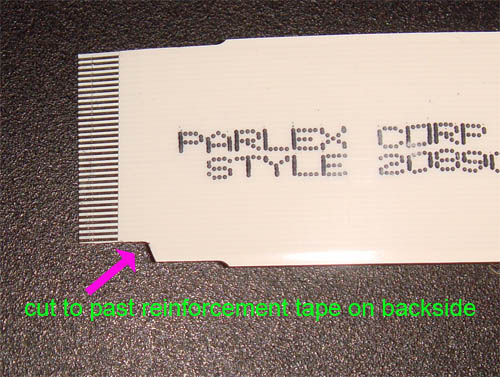
You’ll notice that a 36-pin flat flex cable is specified, even though the Microtips display uses a 33-pin cable. This is because I couldn’t find a 33-pin cable in stock anywhere, but you can use a pair of diagonal cutters to slice a 36-pin cable back into a 33-pin cable. Since there is a chance that you don’t get the cable cut exactly right the first time, I’d recommend buying a couple extra so you can practice on a couple pieces.
Board assembly can be done by hand, although it’s recommended you do it only if you have access to a soldering workstation with a microscope due to the 0.5mm pitch leads on the flat-flex connectors (and use plenty of flux!). Fortunately, microscopes of sufficient quality for soldering work have fallen in price. I recently bought a microscope in China that was a clone of the Accu-Scope 3055 series. While it only costs $100 in China, you can get it in the US for around $260 – about the price of a nice snowboard – and it’s quite a nice microscope for soldering work and performing microsurgery on those nasty hang nails.
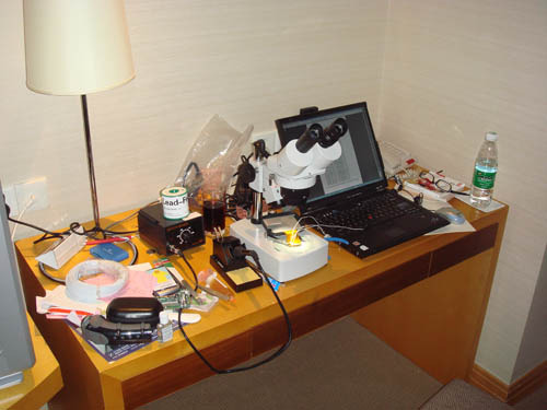
Here’s a picture of the fine-pitch SMT rework setup in my hotel room in China. The neat thing is I was able to buy the whole thing on a Saturday afternoon just wandering around the street markets of Shenzhen, where you find electronic parts vendors cheek to jowl with pushcart stands selling gak and girls pushing fake Chinese tax receipts. “Quick! It’s Saturday and you have to solder 0.5mm pitch wires, but you’re in a hotel room and you need to buy equipment! Where do you go? SEG electronics market!”
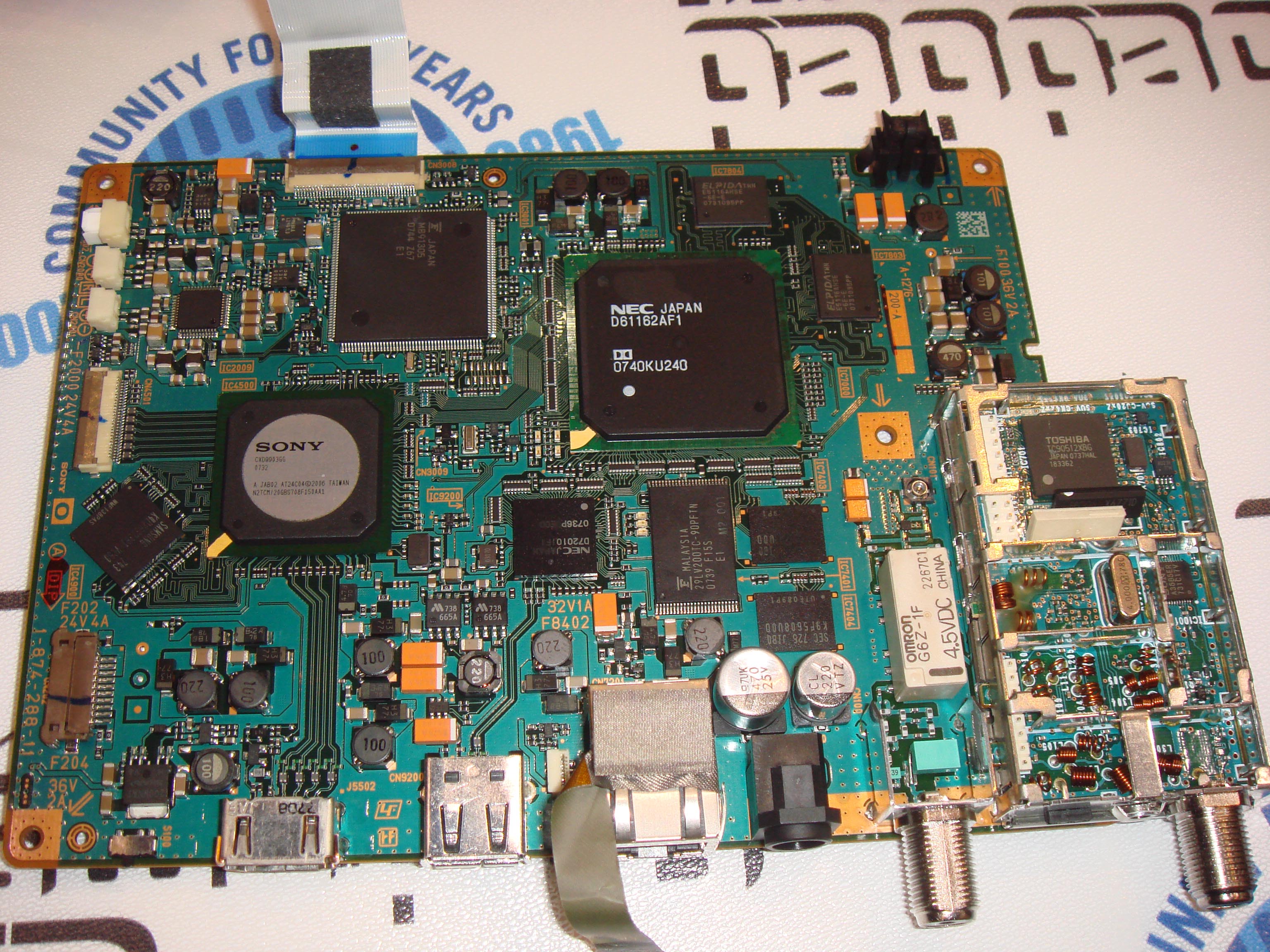
Modifying the Chumby Core
In order to do this hack, you need to sacrifice one chumby. You can take the chumby apart by first breaking the glue seal between the bezel and the soft frame. The easiest way to do this is to pry up on any of the long edges of the soft frame with your finger and start separating the glue bond, and then use a screwdriver or your finger to “chase” the tear around the chumby. If you are careful to always apply the force of the screwdriver or finger toward the hard plastic bezel, there will be no external cosmetic damage to the device and you can reseal it using almost any common superglue (the formulation used by the factory is a little more sophisticated but I’ve had good success bringing chumbys back to “like new” conditions with supermarket-bought superglue).
Once you have the core module separated from the bag, detach it from the ribbon cable. Remove all of the fluffy fill on the inside, and then use a small Philips screwdriver to remove the four retaining screws between the back bezel and the switch/speaker assembly.
You should be able to lift the assembly out of the chumby without much effort. The back bezel should also be stripped off of the leather bag as well, but you will have to peel it off as it is glued in place. When you have all these components out, re-attach the back bezel to the switch/speaker assembly so that the power switch is easily accessible, as the power switch knob is an integral part of the back bezel assembly. Keep all the electronic parts; dispose of the bag and the fill.
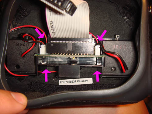
Since you won’t need the old LCD anymore, loosen the two long Philips screws on the wifi riser assembly and liberate the core from the LCD/bezel assembly by detaching the two flat flex cables that connect to the core board. Save the wifi riser assembly, screws, standoffs and cables. Also leave all the thermal pads in place; they will hold on their own if you do not peel them off of the circuit boards.
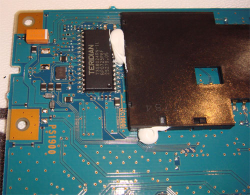
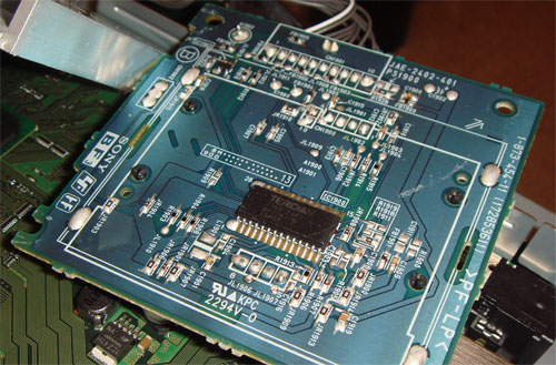
You will need to do some minor rework to the core circuit board of the chumby in order to beef up the backlight driver to work with the more power-hungry backlight of the larger LCD. The original chumby backlight is a 10.2 volt, 40 mA 3-LED backlight. The backlight inside the Microtips LCD is also a 10.2 volt backlight, but it requires 200 mA. Fortunately, the boost converter used to drive the chumby’s backlight has a current switch capable of handling that magnitude of current—the TPS65101 has a 2.3A switch in it. However, some of the external circuitry has to be upgraded. In particular, the catch diode D502 has a forward current rating of 0.5A. While the LCD only draws 200 mA, it is a boost converter so the amount of current going through the catch diode is going to be a bit bigger than the ratio of the output voltage to the input voltage times the average current. Therefore, D502 has to get an upgrade to a footprint-compatible but higher current version, such as the 1A-rated MBRX130TP by Micro Commercial, or the 1.5A-rated RB070M-30TR by Rohm. Finally, in order to actually increase the amount of current pumped into the LCD, the current sense resistor in the feedback network of the boost regulator has to be modified. R524 programs the backlight current in the “on” state of the backlight, though the following relationship: I = 1.146V / R524. Its stock value of 57.6 ohms yields a current near 20 mA; replacing this with a 5.6 ohm resistor will yield a current just over 200 mA.
Replacing D502 is a fairly straightforward task; just be sure to install it with the correct polarity! However, installing a replacement for R524 is a bit trickier. The original resistor is an 0402 sized device that can dissipate up to 0.063W, but the new application requires about 0.25W power dissipation. Therefore, a larger 0805 device needs to be installed. It can be tricky trying to solder a larger SMT component onto pads that are too small for it, so the easiest way to install it is to put it on sideways, spanning between one of the original pads of R524 and the adjacent, connected pad of R525, as shown below.
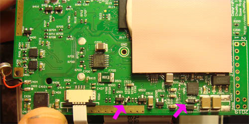
Rework locations are highlighted with the pink arrows.
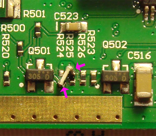
Installation for R524. The 0805 device is kitty corner between its lower pad and the adjacent pad of R525, which is connected to the same signal.
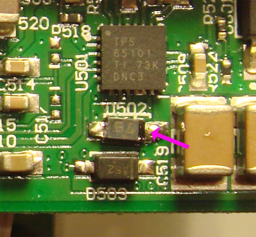
Just make sure you get the polarity right!
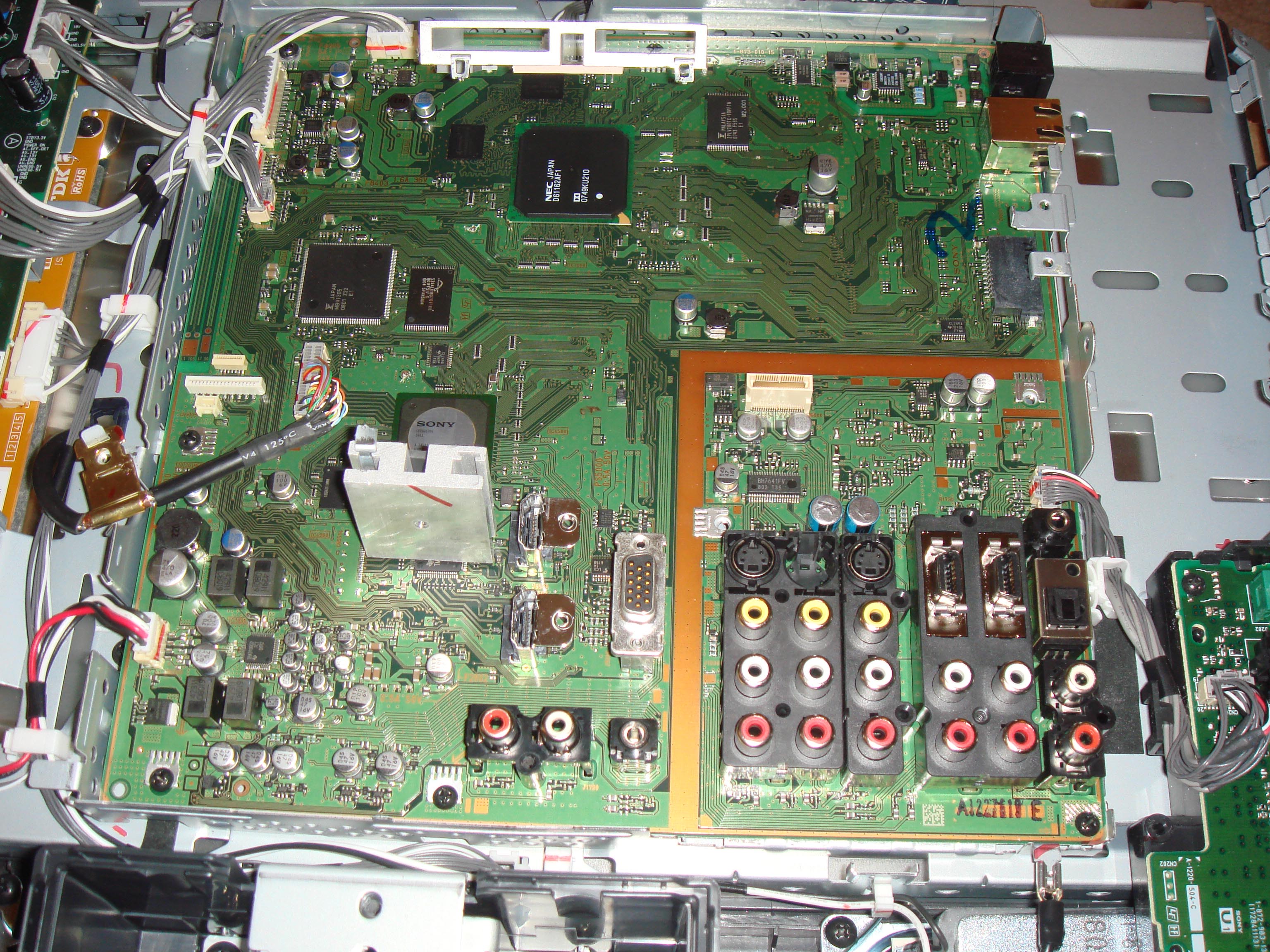
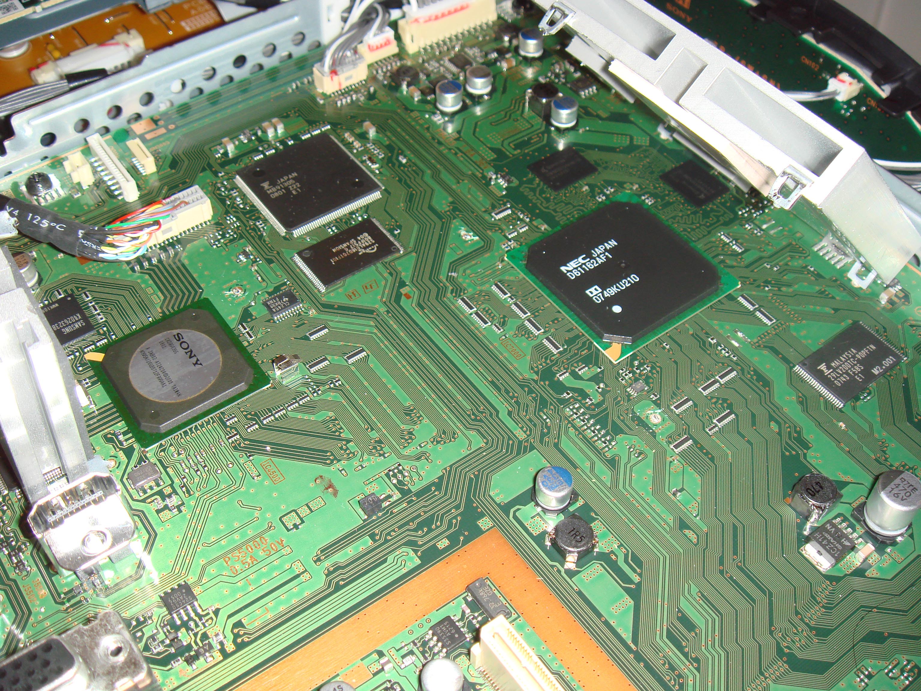
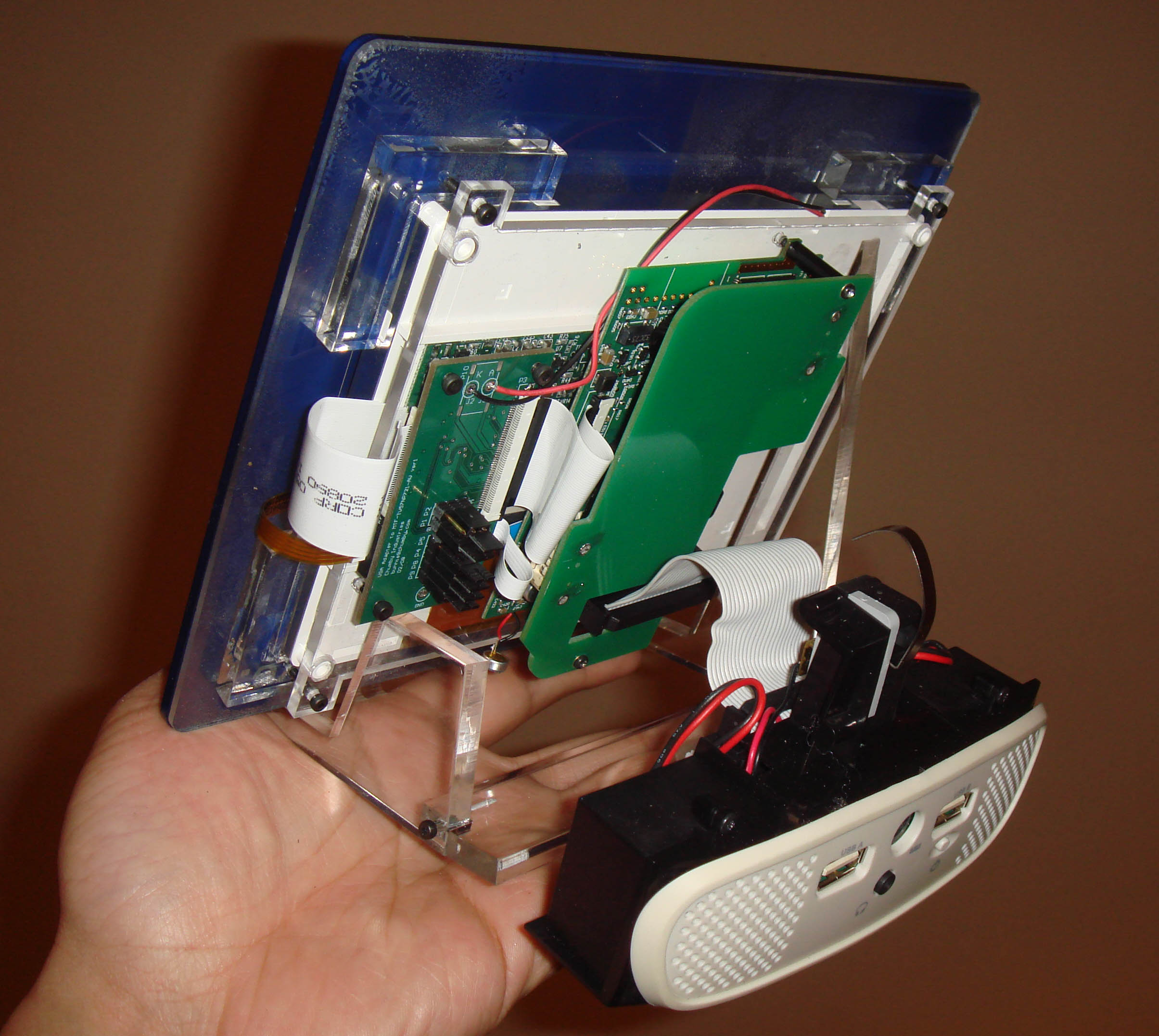
Mounting the Chumby to the new LCD
Now that you’ve got all the bits and pieces, it’s time to put it all together. It’s good practice to mount the pieces so that they aren’t “floating”; the flat flex cables are fragile, and they will easily strain and break if you move the unit around too much. If you have access to a laser cutter, you can build the LCD mount using the designs presented below.
Download all of the designs in Adobe Illustrator format (suitable for printing to a Versalaser VL300 laser cutter straightaway) at this link.

A VL300 lasercutter.
The front bezel could be a simple affair, but I decided to snazz it up a bit by using a process that simulates the look of in-mold decorated injection molded plastics. Normally, with a laser cutter, you engrave on the outside surface, leaving a dull-looking patch and potentially some marring of the work area due to the heat of the laser. In the process I describe here, you first paint the back side of a clear acrylic sheet to the desired color, and then you engrave away the paint from behind. The result is a crystal-clear and mirror-smooth front surface, with a buried color layer and crisp-looking white-colored pattern engraved into the color layer. I finish this off by laminating the back with a second, thin protective layer of acrylic, to prevent the paint from chipping as the piece is handled.
Now, for the details. First take a 1/8” piece of clear acrylic, and strip back the protective shipping tape on one side only in an area that’s about 12″x12″. Immediately spray paint the exposed surface to the color of your choice; in this example, the color blue is used. When selecting a spray paint, pick one that is formulated to adhere to plastic surfaces. Before you spray paint the sheet, it’s important to keep the exposed region free of finger oil, dust and dirt, as these will get trapped underneath the paint and you’ll be staring at those defects forever.
Allow the spraypaint to dry overnight, and then put the assembly into the laser cutter, and load up the front bezel design file.
First, use an engraving-only step (e.g., delete the red lines in the drawing source, or if you are using advanced mode on the laser cutter disable vector cutting) to selectively remove the paint in the shape of the logo you want to have on the bezel. Keep in mind that you are engraving from the back, so the logo has to be flipped about the vertical axis before you do the engraving. You may need to repeat the engraving a couple of times depending upon how thick the paint is, and what color the paint is; in this example, I had to engrave the logo three times before it came out completely clean of dust and dark-colored laser burn products. So before you move the workpiece, take a look at the engraved area and be sure that you can see a consistent, clean sheen of acrylic, free of paint and residue in all areas!
Then, you can cut the bezel out using the red cutting path. Clean the logo regions of any remaining dirt or paint specs using a dry Q-tip and an canned air duster. Do not use a solvent or liquid, as I have found these can get underneath the paint or cause cracking in the freshly cut acrylic.
Next, cut a second protective bezel using 1/16” clear acrylic using the reverse bezel pattern. This pattern also has alignment markers on it, which are important for making sure the LCD’s active area is centered in the opening of the bezel. There is no need to treat the reverse bezel with paint because it is simply a protective layer to protect the painted front bezel from chipping and scratching.
Glue the reverse bezel and the front bezel together using a spray-on adhesive, such as the 3M 3094 Photo Mount Adhesive. To do this, first spray the adhesive onto the reverse bezel (do this on the side without the engraved alignment marks, and be sure to remove the protective plastic layer first) until the whole sheet is frosty.

Then quickly press the two halves together, paying attention to which way the alignment markers should go for the display to be right side up relative to the logos, and hold in place until the adhesive sets. When you are finished, the bezel should look something like this, as viewed from the rear.
Once you have the bezel prepared, cut out the back mounting plate using 1/8” clear acrylic and the backplate pattern.
Finally, cut out the LCD mounting corners and the stand for the assembly using ¼” acrylic and the frame stand pattern.
A set of gaskets are applied to the outside of the LCD along the silvery circuitry area of the touchscreen panel in order to improve the touchscreen’s robustness against heat warpage of the acrylic that can cause the bezel to inadvertently touch down onto the screen. The gasket material in this case is Poron, but you may also use a couple layers of thin-cut pieces of masking tape to create a small offset between the bezel edge and the display.
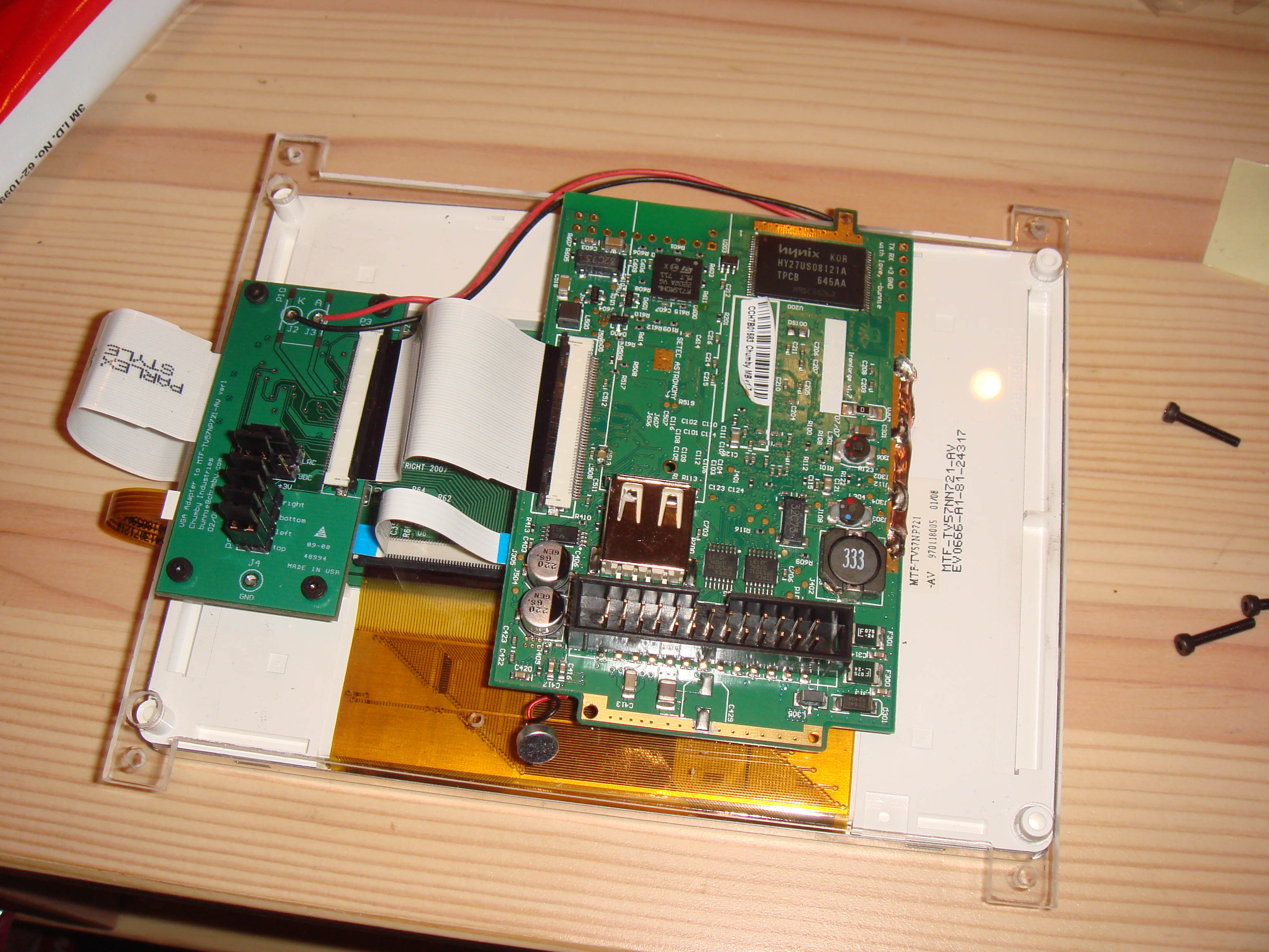
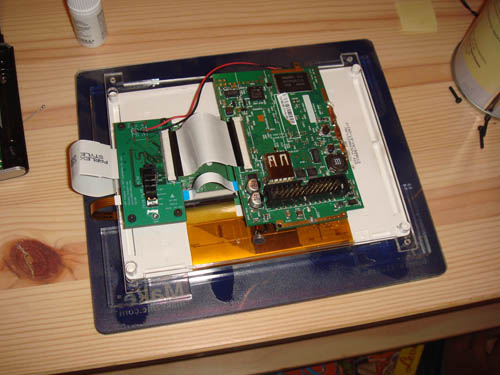
Before screwing the backplate in place, attach the 33-pin flat flex cable (that you previously made by cutting down the 36-pin cable), and connect the other side to the adapter board; at this time, also connect the 4-pin touchpanel cable and the 50-pin cable for the LCD signals to the motherboard. Then, fold the adapter board assembly over and screw it in place using 4x M2x6mm socket cap screws.

(click this image for a larger version).
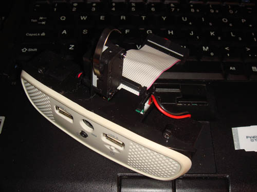
Now, connect both the 4-pin touchpanel cable and the 50-pin flat flex cable to the chumby core board. Screw the chumby core board in place using the original screws, standoffs, and wifi riser.
You’re almost done! Flip the LCD assembly into the bezel, using the alignment pattern on the bezel as a guide, and glue the four LCD mounting corners in place, paying attention to ensure that the holes on the mounting corners line up with the holes on the back plate (you can accidentally put a mounting corner on upside down and have the holes end up on the wrong edge of the LCD). Standard super glue works well for this application. Allow the glue to dry for at least a half hour before proceeding.
Once the glue is dry, screw on the backplate using 4x M2x12mm socket cap screws.
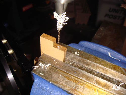
The final step is to build the stand for the display. In order to do this, you will need a drill press and 1/16” drill. Carefully drill holes vertically into the large, semi-rectangular piece with the slot in it as shown below.
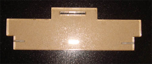
Then, use 2x M2x12 socket cap screws to hold the triangular supports onto the middle piece. One piece has the top of the triangle truncated so that it does not interfere with the adapter board mounted on the backplate. Therefore, take care to make sure you put the truncated piece on the same side as the adapter board!
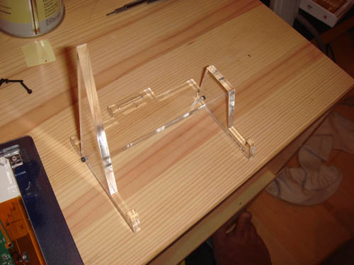
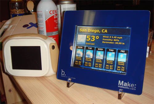
Connect the speaker/switch assembly to the core assembly via the ribbon cable, and prop the whole assembly up on the stand; there is a tab on the speaker/switch assembly that fits into a slot in the stand so the whole unit can be lifted up and carried around without leaving pieces dangerously dangling.

Click on the above image for a larger version.
Modifying the Kernel and Scripts
There’s one more step left in the hack, and that’s to modify the kernel and the boot scripts of the chumby. A stock chumby knows nothing about how to drive a VGA display!
The kernel contains the code that initializes the video frame buffer’s size, so the timing needs to be programmed into these registers by modifying the kernel source. Here is a patchfile that you can apply to the 1.5.0 kernel (build 565) that performs the appropriate initializations. The patch modifies one of the clock registers inside the MX21 to increase the frequency of the clock feeding the LCD controller, and it also modifies the LCD controller registers itself. It also patches code that handles copying the initial logo screen from a staging area in RAM to its final location. It’s more involved to get the bootloader to behave properly and show a more elegant startup screen; here is a link to the modified bootloader source. This code replicates the QVGA bitmaps stored in the bootloader four times over inside the VGA frame buffer for the chumby, and it handles some other corner cases during the hand-off between the bootloader and the kernel at higher resolutions as well.
Now, you need to tell the Adobe Flasplayer inside the chumby to use a VGA resolution when rendering content to the screen. This is done by using the –x and –y command line arguments to specify the screen resolution when the Flashplayer is called. You can use a series of backdoors built into the bootscripts to subvert all of the points at which the Flashplayer is called so that even if the Flashplayer restarts itself due to a timeout or other error condition, it starts with the correct resolution settings (thanks to Henry Groover at Chumby for putting together these scripts!). One of the elegant features of the Chumby Networks’ content is the fact that widgets are typically written using scalable vector graphics in Flash, so for the majority of content, changing the rendering resolution just works and it also looks great.
The following is a link to a USB dongle image that you can use to retrofit your chumby with the above patches, assuming your chumby has previously been updated to firmware version 1.5.0. Download the link, and burn it to a blank USB drive. Then, insert the USB drive into your chumby.
SSH into the device, and execute the following commands:
cd /
tar –xzf /mnt/usb/psp-640.tgz
This operation installs all of the scripts required to override the default settings of the Flashplayer into the read-writeable storage partition /psp.
Finally, reboot while holding down the touchscreen so that you enter the “Special Options” mode. When the selection screen comes up, you should be able to log in via the serial console and execute the command “update.sh USB”, which will overwrite the bootloader and the primary kernel with the code patches mentioned above. For safety reasons, the backup partitions’ kernel is not modified by the dongle, so you always have a safe partition to return to for re-flashing a broken chumby. The graphics on the screen will look funny in this mode, but it’s not harmful for the LCD.
Once the system reboots, you can remove the dongle and enjoy your new high-res, large-screen chumby hack!