This is the second post of a two-part series on Betrusted/Precursor’s True Random Number Generator (TRNG).
A bulletproof source of random numbers is a key component of any cryptosystem, so we’ve done an extensive, months-long characterization of Precursor’s dual, redundant TRNG sources, which consists of an avalanche noise generator and a ring oscillator. We’ve found them to produce passable raw entropy, but you don’t have to take my word for it. You can download our raw data and run your on analysis on it if you like (at least until our ISP cuts us off for serving multiple 10GiB files filled with random data).
However, the system is still missing two features that are generally considered to be best practice:
- Independent, on-line health monitors of the raw TRNG outputs, discussed in our previous post.
- Conditioning of the raw data.
Because Precursor uses an FPGA for its SoC, we can add new features to the hardware “on the fly”, and in this post will focus on adding the hardware for the conditioning of raw data. The post is a bit of a slog to read through; I’ll try not to do too many in this style. But occasionally, I think it’s good to have a “reality check” that conveys the depth of difficulties encountered while implementing a feature, instead of making everything look easy or cramming all the details into a tweet. This post will hopefully also serve as a detailed reference for the handful of future developers who want to implement similar features, and would like to avoid some of the mistakes I’ve made.
Despite best efforts to make TRNGs unbiased and flawless, they are really hard to get right. Furthermore, they are only capable of producing high-quality entropy at a limited data rate. Thus, most practical systems take a TRNG output and run it through a cryptographic stream cipher to generate a final datastream; this conditioning of the raw data simultaneously protects against minor flaws in the TRNG while improving the availability of entropy.
So in Precursor, we’d like to add some conditioning on the collected entropy. To be clear, we will always make the raw entropy pool available for inspection — this is absolutely necessary for testing and CI coverage — but it’s a good idea to throw the output of your TRNG into a cryptographically sound stream cipher of some type, so that in the case that your TRNG suffers a sporadic drop-out, you don’t have a disastrous, instantaneous collapse of entropy. Depending on how you configure the conditioning, you can also increase the effective availability of random numbers.
After poking around a bit on the Internet, it seems popular to feed a seed of entropy into the ChaCha20 stream cipher (I refer to it as a “cipher” in this post, but I think more technically because of the way I’m using it, it should be referred to as a CSPRNG – Cryptographically Secure Pseudo Random Number Generator). This is done in the Linux kernel as well as by cryptech.is’s HSM and a few other implementations. The devil, of course, is always in the details. Cryptech.is takes the output of their TRNGs, hashes them with a SHA2 block, and then feeds it into a ChaCha20 stream cipher. Linux maintains an entropy pool that is collected from a variety of low-and-high-quality sources, blends them using some fast and slow techniques based upon the nature of the source, runs it through SHA1, and then into ChaCha20 to create the final stream.
In our implementation, we’re skipping the SHA pre-hash of the entropy pool, for the following reasons:
- We don’t have the space (as in FPGA gates) or computational resources (as in CPU cycles for software emulation) to do this continuously
- The raw entropy sources themselves are fairly high-quality (as opposed to in the case of Linux they are taking things like time stamps and network traffic patterns, so using SHA-1 to blind that is quite reasonable); and, we have two entropy sources of different architectures, each source consisting of multiple raw entropy generation elements. In other words, we’re starting from a pretty good place already.
- The ChaCha20 cipher is mainly to protect against transient drop-out or unpredicted aging issues in the TRNG.
- The ChaCha20 cipher itself is considered to be cryptographically secure; augmenting it with a SHA pre-hash does not seem to lend any clear benefit in our case.
- We will prefer to reseed the ChaCha20 cipher at a fairly high rate, rather than seed it occasionally through a more expensive SHA operation.
Also in reading some of the docs out there, it seem that 20 is the minimum number of rounds considered to be cryptographically secure for ChaCha, but “more rounds is better”. Thus, while tweaking the Secworks open-source Chacha implementation to fit in Precursor, I think I’ll also create an option to let the ChaCha rounds function run to at least a minimum number of rounds but otherwise “free run” when the system is idle. This makes it useless as a cipher, but if the power impact is minimal, this should help the diffusion of entropy across all the bits of the cipher and make it more robust against attempts to back-track its state.
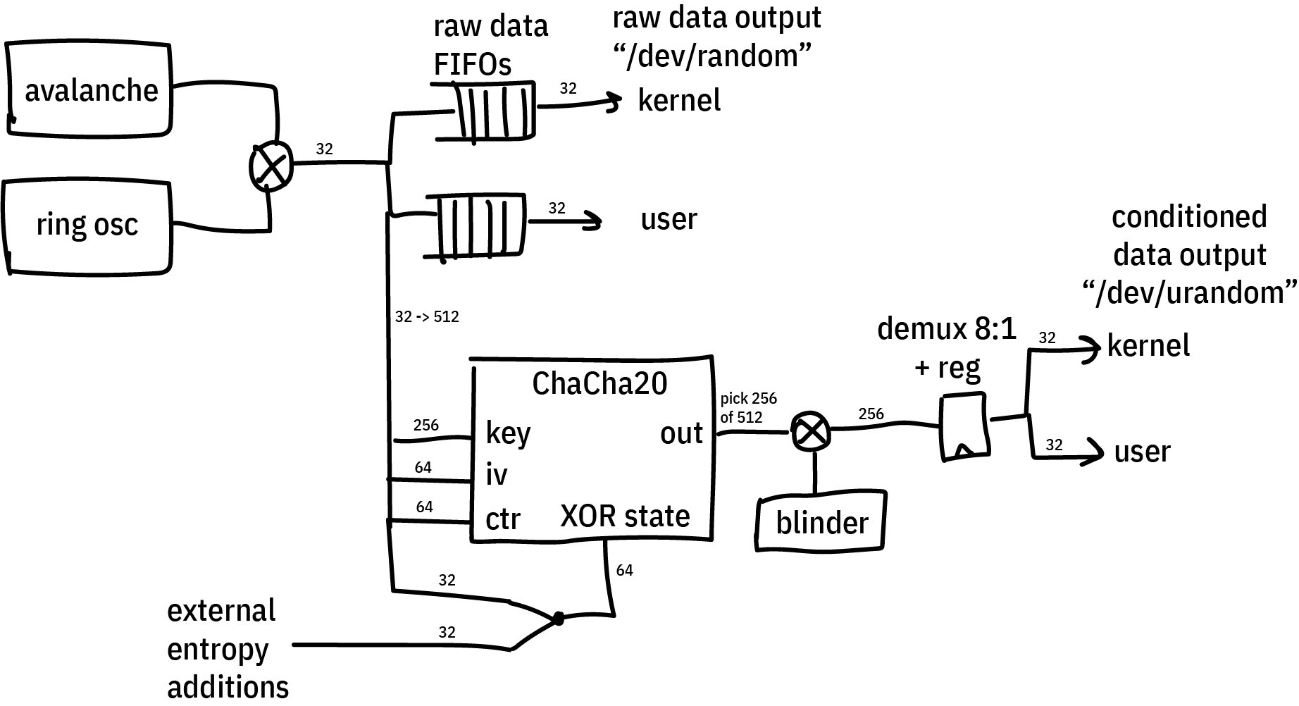
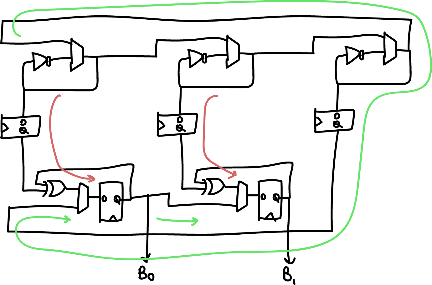
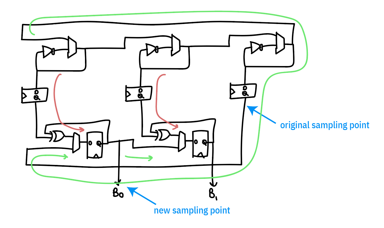
The diagram above gives an “artist’s impression” of the architecture of the system. It’s an early sketch, before I fully understood everything going on. The final details came out a little different, but the big ideas are there. Not shown is logic that ensures the ChaCha20 cipher has completed its minimum amount of rounds between each output sample, and automatic re-seeding logic that pulls in 32 bits of entropy from the TRNGs on a regular basis at some re-seeding interval that can be programmed by software.
After installing the tooling necessary to build a Precursor/Betrusted SoC and run simulations, I started writing the code.
Here’s the general method I use to develop code:
- Think about what I’m trying to do. See above.
- Write the smaller submodules.
- Wrap the smaller modules into a simulation framework that shakes most of the skeletons out of the closet.
- Repeat 1-3, working your way up the chain until you arrive at your full solution.
- Write drivers for your new feature
- Slot your feature into the actual hardware
- Test in real hardware
- Continuously integrate, if possible, either by re-running your sim against every repo change or better yet recompiling and re-running your test on actual hardware.
The key to this loop is the simulation. The better your simulation, the better your outcome. By “better simulation”, I mean, the less assumptions and approximations made in the test bench. For example, one could simulate a module by hooking it up to a hand-rolled set of Verilog vectors that exercises a couple read and write cycles and verifies nothing explodes; or, one could simulate a module by hooking it up to a fully simulated CPU, complete with power-on reset and multiple clock phases, and using a Rust-based framework to exercise the same reads and writes. The two test benches ostensibly achieve the same outcome, but the latter checks much more of the hairy corner cases.
For Betrusted/Precursor, we developed a comprehensive simulation framework that achieves the latter scenario as much as possible. We simulate a full, gate-level VexRISCV CPU, running a Rust-built BIOS, employing as many of the Xilinx-provided hardware models as we can for things like the PLL and global power-on reset. You can make a new testbench by running the “new_sim.py” script in the `deps/gateware/sim` directory, and it will automatically copy over all the basics so you can just instantiate your core module and start running simulation code.
Another thing I learned perhaps too late was to pick a good IDE. Python sucks to develop. It sucks even more without an IDE. For a long time I was writing in vanilla emacs. The game-changer for me was being able to control-click through modules and find their definitions; most IDEs support this.
Writing The Block
I noted in Cryptech.is’s presentations that they were using a 24-round variant with a potential to go to 32; and even though cryptanalysis shows its solid with 20 rounds, perhaps there is still a potential that maybe some knowledge of the output could be used to infer something about the next set of outputs.
So, I still made a very light-fingered change, where the core round function could be advanced by one during idle periods based on a `force_round` input. In any case, the output of the ChaCha cipher is not used until at least 20 rounds in any case, but on average it will go many more rounds (thousands of rounds) before the output is used, and the number of rounds advanced depends upon the exact timing of the code that accesses the TRNG.
Thus, the overall flow of events for the conditioning block are as follows:
- On boot, we pull in 384 bits of “key” state (256 bits key + 64 bits iv + 64 bits nonce) from the TRNG, and then initialize the cipher.
- We also pull in 512 bits of “input” state. This is a fixed quantity that is XOR’d with the ChaCha block state. I worry that tying this to a fixed value could lead to leakage of the ChaCha state to the output, thus, on every boot we load in a new random input value.
- Once the cipher is initialized, a counter keeps track of how many blocks we’ve generated. Once we have passed a threshold, the conditioner automatically requests another 32-bit word of entropy from the TRNG and does a rotate-and-XOR of the data into the “key” state. The key state is re-incorporated on the next “advance” call of the block.
- Every “selfmix” interval, the cipher will also advance its rounds counter by one (this is the supplemental entropy/scrambling as noted previously)
- The user can also supply seeding data at any time, which is folded in with a rotate-and-XOR function. Note for every seed provided, it’s best practice to read 16 words of TRNG output, to ensure that the seed state is incorporated into the TRNG as a whole. It doesn’t harm things to not do that, just, if you kept on applying the same seed over and over again it’ll eventually just XOR into and out of the key pool without doing anything useful.
- The output of the cipher is latched into a 512-bit register, and `urandom` data outputs are multiplexed to the kernel and userspace through the CSR. A `valid` bit is provided, and it should be checked prior to every read of data from the Conditioned TRNG output.
Building, and Failing
So your code is all writ, now time to try a quick “smoke test” to see if the build fails. And, sure enough, even though the build completes, I’m not meeting timing. We’re using a -1L variant of the Spartan 7 part, which is the lowest power model (important for battery life) but also the slowest performer in the group. So, even though Cryptech.is advertised hitting 100MHz performance on the block, I did note they were using a -3 variant (one of the fastest models) of a fairly high-end Artix FPGA.
So, back to the drawing board — it’s time to drop the clock frequency on the core to 50MHz. This is probably fine from a performance standpoint, as it could still yield 1.6Gbps burst rate of random numbers, but it does introduce some potentially thorny issues with clock domain crossings. In particular, I don’t get to be lazy and just use a bunch of Migen’s BusSynchronizer primitives to bridge 512-bit data between domains. That would be…expensive, in terms of logic resources. Instead, I’m going to have to be careful and use multi-cycle paths with explicit timing exceptions to make sure this works and without consuming undue amounts of resources.
What — you mean you thought getting code to compile was the end of the story? In hardware, every flip flop is a race condition against a clock — just think of it that way. Every time you make a register, you now have a potential concurrency problem. Now scale that up to the tens of thousands of registers in an FPGA, and you get an idea of why correct compilation is only a small portion of the whole story.
Failing More, in Order to Get Better
After reducing the frequency of the core to 50MHz and fighting for a half day with the Vivado constraints syntax to convince it not to spend half an hour routing cross-clock-domain that are actually relaxed, I finally have the design building with timing closure. The next step is going back into the simulation bench and checking all the corner cases.
I modified the existing `trng_managed` simulation bench to add a series of tests that would exercise all the new features — including checking the rate of read, all the dual port options, and deliberately forcing some reads to fail by bypassing certain checks on validity of data to really push the engine to its limit. In the process of running these benches, I found more new corner cases, for example, the ChaCha engine would stall if the raw entropy FIFO ran out of seeding data; it would just wait for reboot of the avalanche+ring oscillator TRNGs, a process that can take milliseconds. This shouldn’t happen on the `urandom` engine — it is the “unlimited” random data engine after all, so some fixes were made to keep the block state evolving even if we ran out of seeding data. However, I have to emphasize this really is a corner case, you have to basically configure the system to constantly reseed and pull entropy out at a rate much higher than you can do anything useful with it to hit that limit. But, that’s the point of testing — to break your system before users do.
Rinse, Lather, Repeat
Now that the simulation runs, we repeat the loop and see how badly timing is broken. It turns out with all the tweaks in place, I’ve introduced an accidental critical path. While the design can meet timing with this, it takes almost 3x the time to build, which means we’re probably going to start failing builds pretty soon. I should probably fix this problem now, while the design details are fresh in my head.
I open up the design in the Vivado tools and have it plot a timing histogram for me, below is an example of the output:
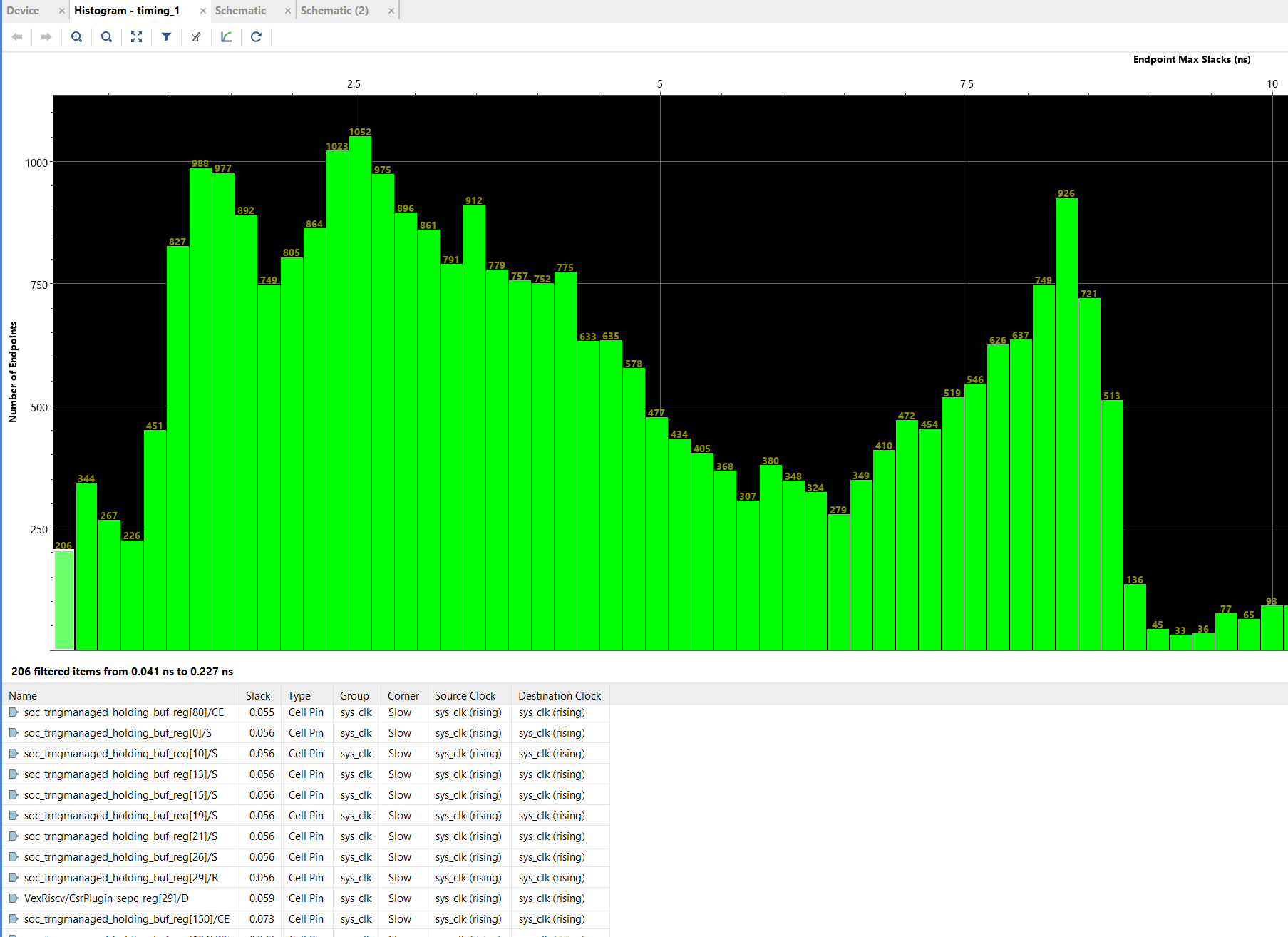
Above: Example of a slack histogram generated by Vivado. Green bars toward the left indicate paths with less timing slack, to the right have more. So for example, the left-most bin has 206 paths with 0.041ns-0.227ns of slack. The more “left-heavy” the histogram is, the harder the design is to place & route, and the more likely the process will not complete with perfect timing closure.
The left-most bin are the most over-constrained elements, and I can see that the `trngmanaged_holding_buf` registers are just barely passing.
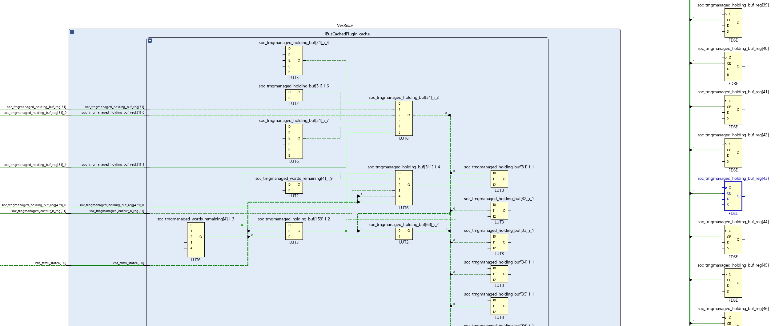
I generate a schematic view like this inside the Vivado design tool, and backtracing the inputs to the `holding_buf` registers I can see the signal eventually goes through an enormous combinational path that includes the VexRiscV’s address decoders. This means that we have a critical path that extends from inside the VexRiscV load/store unit all the way to the 512-bit shifter of the ChaCha block.
If it were the case that we actually needed to pull data cycle-by-cycle out of the ChaCha block and somehow change the behavior of the system within a single cycle, then this path would make sense. But in practice, the actual rate is far lower than that — the tightest, most unrolled read loops take at least 2 cycles to execute; but more typically 10-12 cycles per iteration if you’re doing any sort of useful load or store with the data and running it from a rolled-up loop. Furthermore, the ChaCha block is basically a “read-only” block — there’s nothing the CPU is going to do to reconfigure it on the fly that would prevent us from
pipelining this.
So, I go back and add a “depth 1 FIFO” to the output, to break the shift register out of the critical path while still preserving the read-invalidate semantics required by the CSR interface (that is, the contract we have with the CSR interface is the cycle after a random number is read, either the next value should be a valid, new random number; or it can be an invalid number, but the “valid” bit must be cleared that very cycle). Using a simple pipeline register won’t work, because it introduces an extra cycle delay on the read-invalidate semantics and it’s possible, although very unlikely, that a code loop could have back-to-back loads and it will grab a stale “valid” state.
After running another simulation just to make sure we haven’t introduced any new bugs, I run a compilation again and hope this greatly relaxes the timing. It didn’t, but long story short, I had accidentally leaked one path in the FIFO through as a combinational element. After spending a couple hours tracing that issue out, I finally met with some success.
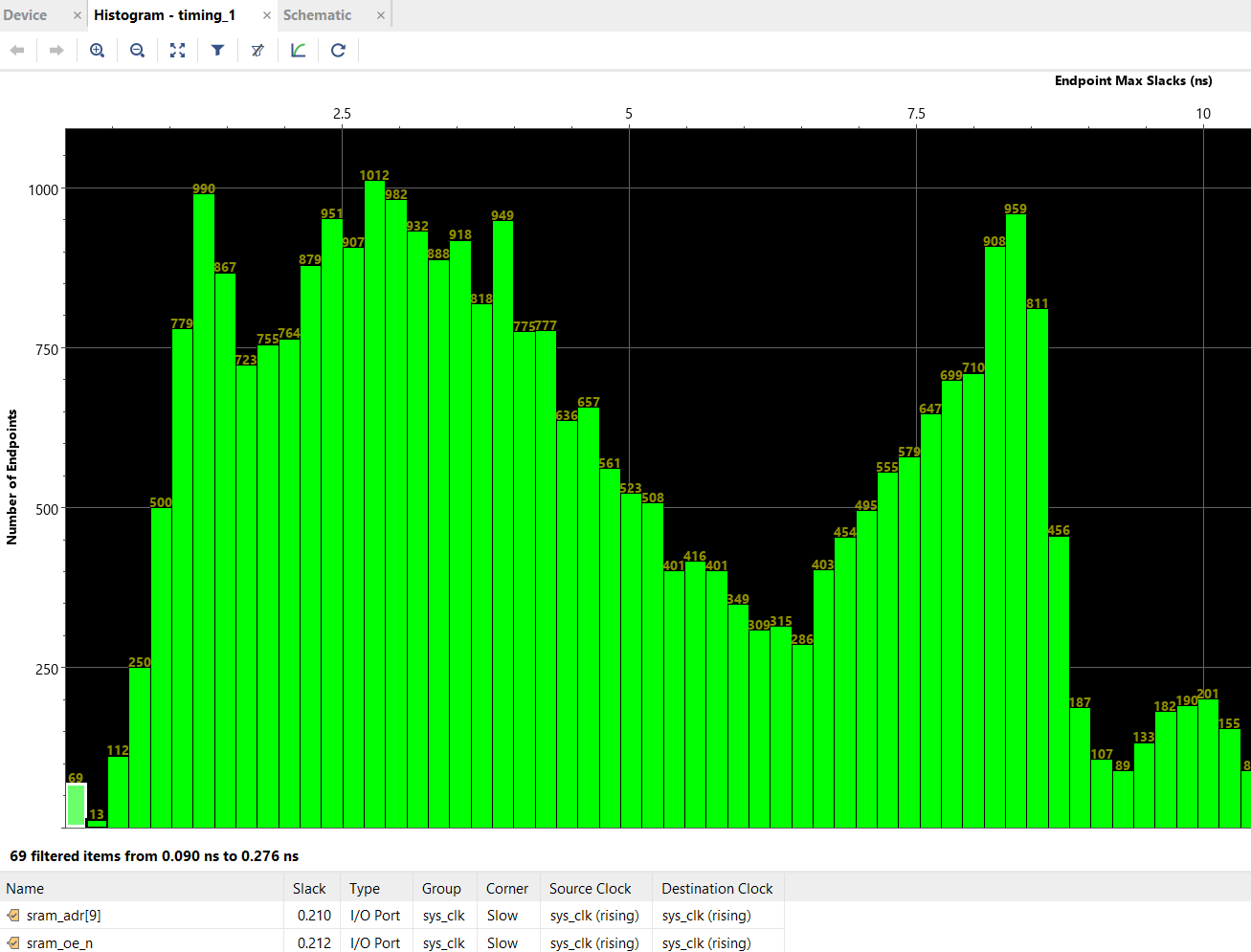
After applying these fixes, the compilation time is back down to its normal value, and we can see that the timing bins at the very far left of the histogram have a fraction of paths as before — 69, down from 206. It looks like the `holding_buf` register is still causing some troubles, but at least we’ve taken pressure off of the actually most difficult paths, which are inside the Curve 25519 Engine, and not some made-up timing emergencies inside the shift register at the output stage of the TRNG.
The price of all the timing fixes is increased resource utilization. Initial estimates showed about a 6% area cost for the ChaCha block without the timing fixes, but we ended up with around 10.5% area cost once all is said and done. The SoC uses around 68.2% of the FPGA now, which is still fine for routability and gives some space for a few more smaller blocks, but it’s probably at the upper limit of what we can reasonably expect to fit while having short (~8-9 minute) compilation cycles. I’m also making a mental note to myself that as part of the histogram analysis it looks like the next critical path to knock back is in the CSR address decoders. Adding the dozens of registers to read out the results from the TRNG health tests has probably forced an extra layer of LUTs to be instantiated inside the core arbitration logic; thus, pruning some of these registers if they end up being superfluous could be a way to win back some timing margin if I end up in a jam later.
Rubber, Meet Road. Road, Meet Rubber.
Well, that took some time in simulation. But we’re not done yet! It’s time to run this code on real hardware, and then upgrade the kernel and services of Xous to use it — and let’s not forget CI integration as well.
First things first, let’s just take the design, as-is, with no mods to Xous and see if it boots, and what the power draw change is. The good news is that things boot, and the system draws about 5 mA extra, or about 5% more idle power than it did before. The ChaCha whitener is in the always-on domain, because it has to be able to run while the kernel is idling to produce random data. In particular, the core can “wake up” the avalanche generator and ring oscillators while the CPU is idle to summon more TRNG data even when the CPU is asleep; as such its clock can’t be gated off, but it is better than the alternative of running the CPU to manage these processes. A quick test tweaking the knobs on the duty cycle of the self-mixing for the ChaCha core shows it doesn’t have a measurable impact on the power, which means that probably most of the extra power is just the fixed cost of clocking that much more logic on the fabric.
The next step is to switch over the kernel and core services from using raw random numbers to the new ChaCha conditioned “urandom” source. This should have been easy in theory since everything worked in simulation, but of course — it didn’t work. I was greeted with a full system hang on the first go. This kind of bug is dreaded, because it’s some issue in the full system integration that exists outside of the testbenches, so you have to resort to long compile cycles and “printf” debugging.
Some further poking revealed that even worse yet, on some boots, the system worked, on others, it didn’t. However, the pattern was enough for me to suspect an issue in the reset logic. Going back into my code, I did find a subtle bug where I forgot to assign the reset line for the ChaCha core to the 50MHz clock domain (it was still tied to the reset for the 100MHz clock domain). For good measure, I also added a reset pulse extender, just to make sure it saw a long, solid reset. The polarity of the ChaCha core reset is opposite from what the rest of the system uses, so it’s also possible there is some glitches due to that. Anyways, after another four hours of tweaking and testing these fixes, re-running simulations, and cross-checking documentation about the reset process to really make sure we found a root cause, the system seems to come up as expected from the “urandom” source.
For TRNGs, The Work is Never Done
The final phase of modifying any TRNG is continuous integration. This is extremely important because you can only get a hint if a TRNG is mis-behaving in subtle ways after collecting dozens of gigabytes of data from it over dozens of runs; and due to the limited rate of entropy, gathering such quantity of data can take weeks. Thus, we have a Precursor unit dedicated to doing nothing but rotating through its entropy sources and feeding its data into a set of test suites to try and uncover any subtle biases in the generators. You can browse the raw data and results of our CI bench here.
Now that we have this conditioned output, we need to integrate that into the test bench. It’s also going to be important to do a few “cold boot with recorded data” runs as well, so we can compare boot-to-boot to make sure that we have actually seeded the generator with random data and we’re not just accidentally running a ChaCha cipher (which should have excellent statistical randomness) with a fixed set of keys (which would have an identical stream boot-to-boot despite the excellent statistics).
In the process of re-integrating these tests into the CI bench, I discovered a number of problems with our original tool for shuttling random numbers to the host for analysis. For a number of reasons, the original CI tool relied on a fairly complicated Rust program with multiple threads, which was getting hard to maintain and the Rust wasn’t adding a lot of value; in fact I found a subtle integration bug that was causing all the tests for the past month to be run only on the ring oscillator!
Since we had a pretty decent Python script for doing USB updates over USB, I modified that into a script currently living in xous-core/tools/trng_test.py. This script is matched to a thread that runs inside the `trng` server on the Xous side when it is built with one of the TRNG tester options. On the Precursor side, a pair of 512kiB buffers are filled and the host is told which of the two to read from. The host-side Python script then reads the buffers and echos its contents out as binary data to stdout, which can then by piped into an analysis program (such as `dieharder`) or recorded to disk for later analysis. This whole mess is then wrapped in some other shell-script Frankenstein that’s fired off by a cron job which manages the rebuild, reflashing, and logging of data via a Raspberry Pi that can keep an eye on the serial console for errors during the CI process. It feels like a house made of playing cards, but it works!
Closing Thoughts
If you made it this far, congratulations. Hopefully it conveys, with some accuracy, the range of difficulties one might encounter when implementing a “typical” feature like this for an FPGA-based SoC, and it may even be useful to the handful of developers who want to actually attempt something like this!