While the last few updates about Precursor have focused on evidence-based trust and security, this update is more about the process of making Precursor itself. There is an essential link between evidence-based trust and understanding the manufacturing process: to convince yourself that something has been constructed correctly, it’s helpful to understand the construction process itself. It’s hard to tell if a small crack in a wall is the result of harmless foundation settling, or a harbinger of a building’s imminent collapse, without first understanding the function and construction of that wall.
Most designers like to abstract the PCB away as a commodity service, preferring “no-touch” or “one-click” ordering services where design files are uploaded and finished boards arrive in the mail, on time and at a good price. This is a bit like running a restaurant and ordering your produce from a mass distributor. The quality is uniform, delivery times are good, and the taste is acceptable. However, it’s hard to make a dish that’s really differentiated when basic ingredients all come from the same place.
I personally enjoy building electronics with a bit more of an artisanal flavor. Just as gourmet chefs invest the effort to develop relationships with their farmers, I’ve developed a personal relationship with my preferred PCB shop, King Credie. Since a PCB is at the core of virtually everything I build, I have found developing a healthy personal relationship with my PCB supplier has the benefit of raising the bar on virtually all my products. While King Credie is neither the cheapest nor the quickest-turn of PCB shops, their quality is consistent and, most importantly, they are willing to customize their process. For a small shop, they offer a wide variety of speciality processes, such as rigi-flex, metal core, edge plated cavities, HDI, and custom soldermask colors.
The Precursor Bezel
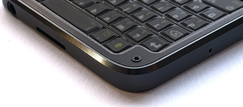
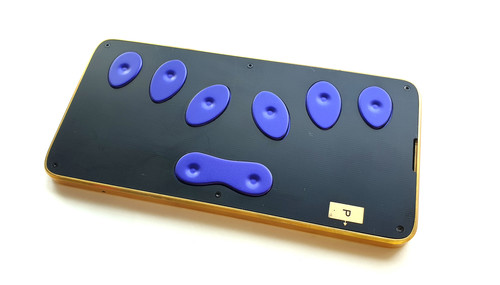
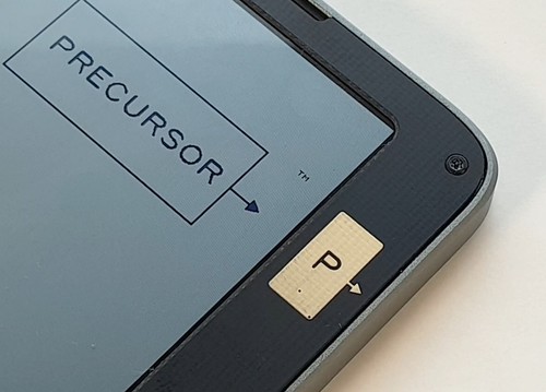
The bezel for Precursor, shown below, is a good example of how this flexibility can be used in practice. The front surface of Precursor is actually a raw FR-4 PCB while the Precursor logo is a 2.4GHz antenna. The two small black dots in the logo beneath the “P” are the antenna feed and ground stub vias, respectively, for a “PIFA” (planar inverse F)-style antenna. The PCB itself has been countersunk, beveled, and step-milled so it can function simultaneously as a mechanical bezel, an RF antenna, and a circuit board for electrical components.


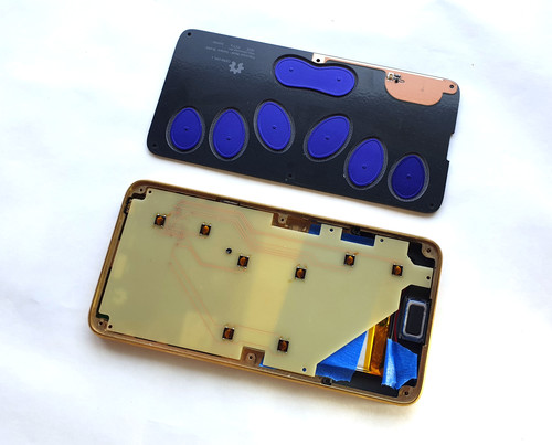
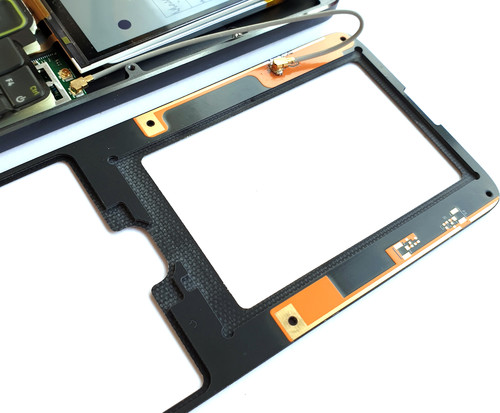
Above is an inside shot of the bezel displaying step-milling and electrical circuitry on the inside surface of the bezel PCB. The back side components are for antenna impedance matching circuitry, connector, and ESD protection. A shiny layer of clear soldermask is applied, and you can clearly see the glass weave that forms the structure of FR-4 in the step-milled areas where material is removed. This constrains the LCD’s location and makes space for cables and keyboard components.

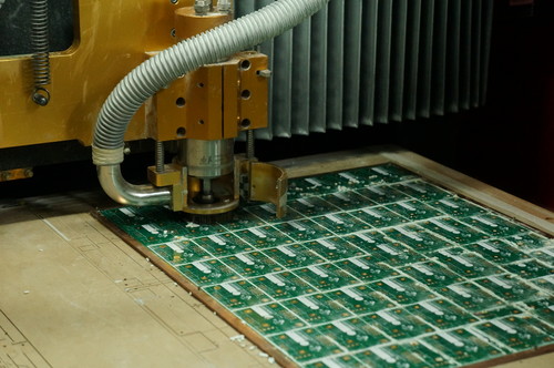
Example of a milling machine at King Credie (image courtesy Chris ‘Akiba’ Wong).
Although step-milling and countersinking are not considered “standard” processes for PCB manufacture, it turns out that all PCBs go through a milling (or routing) process anyways. This process defines their final shape by cutting them out of a larger mother panel. Above is a photo of such a machine doing edge routing. Here, the PCB panels are stacked about five or six panels high and a routing bit is defining the final outline of each of the smaller PCBs. Since the PCB shop already has several types of precision CNC machines that can do both routing and milling, getting countersinks and step-milling done is mostly a matter of buying the correct bits and convincing the shop to do it.
That last point is tricky: since most PCB shops compete solely on price, any disruptions in tooling can lead to costly mistakes. For example, if a machine was configured for countersinking but then the operator forgot to reconfigure it for routing, the machine might have the wrong bit installed for the next operator, and a whole panel would be lost at the final stage of production! Thus the risk of small process tweaks can be amplified by ripple-effects onto other volume processes.
Fortunately, King Credie has a pricing model where they largely separate the cost to set up a manufacturing run from the cost of production. Thus, for a highly bespoke PCB like this, I might pay a few hundred dollars to set up a production run, yet just a few bucks for the raw FR-4 material. The good news is that once the new process is finalized, the cost amortizes well over a production run the size of Precursor’s.
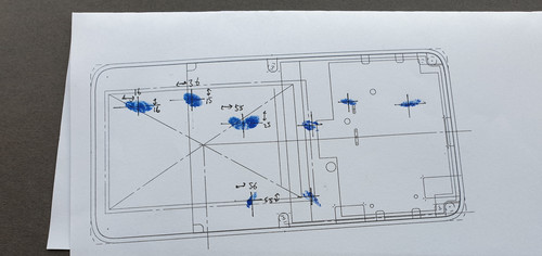
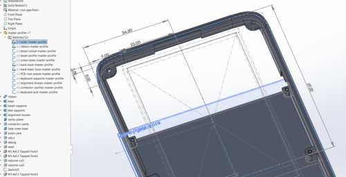
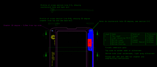
Of course, specifying such a bespoke processes is also a challenge. There isn’t a standard (that I’m aware of!) for communicating these types of things to a PCB shop, so I’ve mainly resorted to ad-hoc drawings on mechanical layers in my design tool.

Above is an example of how the bezel is specified to the manufacturer. Because of the complex 2.5D topology of this PCB, I also include several cross-sections to help clarify the drawings. I also try to make it so that the gerber lines are specifying either direct tooling paths or keep-outs (as opposed to using fills and polyregions and leaving it up to the shop to define a tool path within these regions).

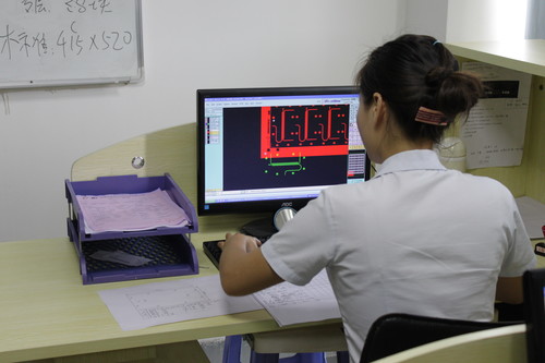
Above: A King Credie engineer reviews and edits a customer’s design (image courtesy Jin Joo ‘Jinx’ Lee).
Of course, there’s a lot of email back-and-forth with the PCB shop to clarify things, and it takes an extra week to process the boards, But, it’s very important not to rush the shop when specifying highly bespoke designs because you want the best machine operators to run your boards, not just the ones who happen to be available that day. When things get really challenging, I know that King Credie’s CEO will personally go on the line to supervise production, but this is only possible because I let them prioritize correct results over fast turn delivery – he’s a busy guy, but it’s well worth the wait to get his personal assistance. He’s an engineer at heart and he knows the company’s capabilities like the back of his hand. And finally, it helps if I make it clear to the shop that for risky production runs like this, I will pay 100% of the quoted price, even if the scrap rate is high and they can only do a partial delivery. That being said, I’ve rarely been in a situation where the shop has had to adjust delivery quantities because of yield issues. I was lucky in that the bezel process worked on the first try (subsequent iterations were around refining the antenna shape and cosmetic details), but I’ve definitely had challenging PCBs where I’ve had to pay for two or three goes at process development before I had a process that worked right and yielded well.
The Precursor Mainboard
There’s another aspect of PCB manufacturing that is fairly ubiquitous yet surprisingly rare in the open source hardware world: microvias.

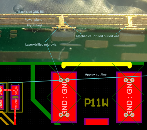
Above is a cross-section view of the Precursor PCB, lined up against a design view of the same. Here, the PCB has been cut through a ground pad for the wifi antenna, showing a stack of two laser-drilled microvias on top of a mechanically drilled via. As you can see from this image, two microvias can fit side-by-side in the area of a standard mechanically drilled via. To put it in solid numbers, the microvias here have a hole size of 0.1mm and an annulus of 0.2mm; and the mechanical via has a hole size of 0.25mm and an annulus of 0.5mm.
This style of via is absolutely essential in handheld products with space-conscious packaging featuring typical pitches of around 0.4mm for balls on a WLCSP.

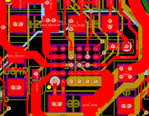
Above is an example of one such WLCSP used on Precursor. The distance between each of the small round pads above is 0.4mm. You can see clearly here the contrast between the size of the mechanical drills and the laser-drilled microvias, and how essential they are for reaching the inner ranks of balls for these tiny packages.

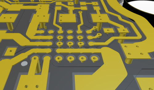
Above is the same rough area of the PCB, but rendered in 3-D and highlighting the top layer only.

And above is the same area once again, rendered at the same angle but showing the second layer, underneath the top layer. These renderings help give an intuition for the relative scale and size of a microvia compared to a conventional mechanically drilled via.
I say that microvia technology is ubiquitous, because we all own at least one gadget that uses it liberally: our smartphone. Even the cheap $20 smartphones from the Shenzhen markets use microvia, so clearly it is a mature volume technology. However, very few open hardware products use it; to the best of my knowledge, Xobs’ Fomu was the first. My best guess as to its lack of popularity in open hardware is the high setup cost for microvia. But the high setup cost is driven in part due to a lack of demand and thus you have a classic chicken-and-egg problem blocking technological progress in open hardware.
As essential as microvia boards are for mobile gadgets, they are more expensive than through-drilled multi-layer boards for a few good reasons:
- Laser drilled vias can only penetrate about 0.1mm thickness of material. Thus, they are almost always paired with a mechanical drilling process to get signals through the full thickness of a board.
- Although drilling a single laser via is faster than drilling a mechanical via, a mechanical drill can penetrate several copies of the board at once, thus reducing the comparative speed benefit of laser drilling.
- This combination of drilling processes means the board material has to be taken off the line several times for drilling operations, instead of being etched, laminated, and then drilled only once.
- Stacked vias are almost always required with microvia designs and thus even the mechanical vias have to be filled in with copper to allow via stacking (normally they are left hollow in a regular multi-layer board).
- Although mechanical drill bits must be replaced regularly, they can be recycled and reconditioned. Counter to my intuition, I was told that lasers (despite being solid-state) also wear out and require expensive periodic maintenance, particularly at the high power levels required for drilling.
- Laser drilling is done with an X-Y CNC head, not with a galvanometer system as I had previously assumed, which significantly reduces the potential speed advantage of using light. Apparently this is related to the difficulty of keeping the laser focused over the entire dimension of the PCB and also the need to keep the drill hole vertical. I’m guessing there are probably more advanced laser drilling machines than the one I’ve seen which use a parabolic mirror with a single galvaonometer axis (similar to the Form 3).
Despite these extra costs, it’s virtually impossible to make a handheld gadget these days without microvia technology. The entire parts ecosystem for mobile devices assumes access to microvia technology, Without it, you just can’t access the latest technology in chargers, regulators, and other ICs.

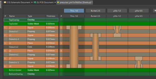
Above is Precursor’s microvia “board layer stack” as seen in my design tool. It’s a 6-layer board. I have just two microvia layers (“top” uVia 1:2 and “bottom” uVia 6:5), paired with two types of mechanical drills, one which is a “buried” 2:5 layer and a “thru” 1:6. This type of layer stack is about the simplest microvia stack you can order (you could forgo the buried 2:5 layer, I suppose), but even this simple stack makes routing even the tightest 0.4mm BGAs in Precursor so easy, it almost feels like cheating.
In case you’re having trouble visualizing how this all comes together, I ordered a special run of Precursor boards from King Credie, where they pulled the material at each key process step so I could scan it and show you what the board looks like as it’s being made. (For the record, they did not sponsor this post – this post was my idea and I paid for all the extra PCB material that made it possible.)

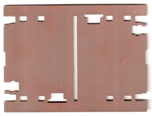
All boards start as a uniformly copper-clad piece of FR-4 material, like the pieces shown above (image courtesy Akiba). Boards are built from the inside-out, so in the case of Precursor it starts with a piece of FR-4 that is about 0.23mm thick, with 0.018mm thick copper on either side.

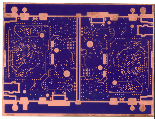
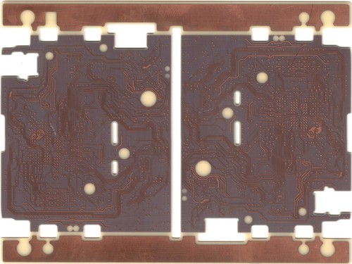
The first step is to photo-image the inner layers, which in the case of Precursor are predominantly ground and power planes. The purple areas above are a thin layer of photoresist applied on top of a uniform copper foil layer.

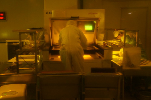
Above: photo-imaging is done in a cleanroom with special lighting to avoid exposing the photoresist (image courtesy Akiba).
The photoresist protects the copper from being etched. The copper is chemically etched and the photoresist stripped, leaving just the etched copper pattern.

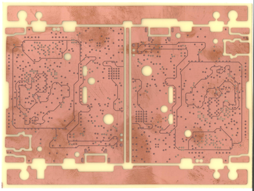
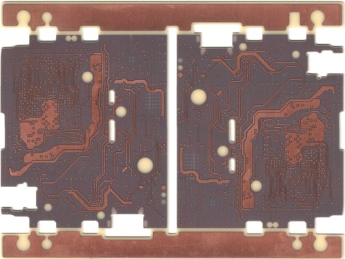
Above is the inner power layer of the Precursor PCB after etching and photoresist stripping. At this point, the PCB process is identical to that of a typical two-layer PCB.
After the inner layers are defined, the final “board stack” is created by laminating alternating layers of FR-4 and copper foil together.

Above is an example of a six-layer PCB stack (it’s not the exact one used in Precursor, but it illustrates the idea adequately). The yellowish material in between the copper layers is called FR-4, an epoxy-impregnated glass – basically, a type of fiberglass, the same kind of stuff used in Corvette car body panels and lightweight boats, which is why we can also use it as a structural material for the bezel of Precursor. The only difference for Precursor’s bezel is that a black dye is added to the base FR-4 material. A typical use for black FR-4 is in free-space IR technologies, such as remote controls, or front panels of equipment with LEDs inside, where the ability to fully block light across a wide spectrum can be important for functional reasons. But, in the Precursor bezel, we use the black color solely for aesthetics.
The “FR” designation stands for “flame retardant”. The PCB shop purchases it in two forms, one is called “core,” the other “prepreg”. Core FR-4 material is cured, so it is harder and stiffer; it’s basically the stuff inside your basic two-layer PCB. Prepreg is a “pre-impregnated” sheaf of glass fiber with epoxy. Since the epoxy has not been heat-cured, it’s substantially more flexible than core material, typically thinner, and can come with or without foil on one or either side. The prepreg is essentially a glue layer that is used to bind the copper layers together.

Once stacked together, the raw PCB material is put into an autoclave which heats the assembly to over 175C (~350F) while applying over 20x atmospheric pressure for about an hour. Above is an image of such an oven, where the hydraulic press racks are stored on the right, and the oven is in the center-left. During this process, the prepreg cures into its final, hardened form, flowing over the etched copper traces to fill all the voids.
Significantly, this pressing process reduces the overall thickness of the PCB. This is a very significant factor for applications that require impedance control or tight finished thickness control. Specifying buried impedance-controlled layers thus requires an additional step of analyzing the amount of pre-preg that flows into the voids between copper, because this affects the final distance to the adjacent ground planes and thus the final impedance. No board design software as far as I know accounts for this, because the physics of this flow depend heavily upon the specific precursor materials used. Thus, it’s important to send impedance-controlled PCBs to the PCB shop for analysis, so that final trace widths can be adjusted prior to tape-out for an accurate finished impedance.

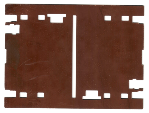
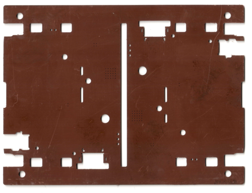
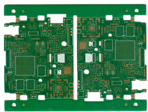
In the case of Precursor, an extra layer of pre-preg + copper is added to either side of the two-layer core, creating a four-layer PCB structure as shown above. At this point, the coarse board outline routing structures are defined. This includes the gaps for processing rails, through-hole components, and mounting features. Alignment holes to assist with alignment for future process steps are also added in the material outside the finished panel. Although the structure above looks like a blank PCB, it in fact already holds the internal ground and power planes! This is an important fact to keep in mind when contemplating the potential for this process to hide implants within a PCB laminate stack.
The PCB then goes through a pass of mechanical drilling, plating, etching, and hole back-filling, ending up with the four-layer PCB structure shown below.


The above shows the top and bottom sides of the inner four-layer stack of Precursor. Mechanical through-holes have been drilled, but notice how they have been completely back-filled with copper so that there are no voids, allowing us to stack microvia on top of the mechanically drilled holes.
If we were making a conventional four-layer PCB, we’d be done at this point! But, because we’re doing microvia, the PCB has to make yet another pass through the PCB shop’s laminate-etch-drill process. Any yield defects after to this point start to get very expensive, so the PCB shop has to have its process control spot-on to build a microvia process.
The Precursor PCB gets yet another extra layer of prepreg + copper laminated on, so it once again looks like the “bare” PCB photo shown a bit above, then it’s sent into the laser drilling process.

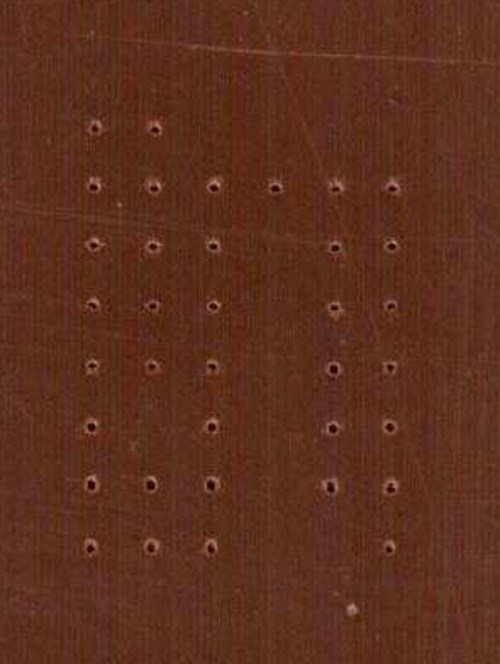
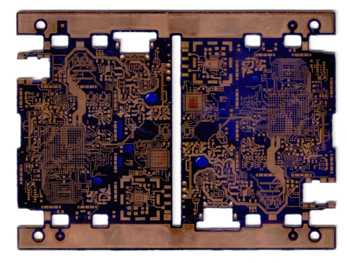
After the laser drilling process, you can barely see the tiny 0.1mm holes pitting the surface of the copper, which is now dusty with a reddish-brown protective oxide layer naturally resulting from the lamination process. I believe the protective layer also assists with the adsorption of laser radiation for more efficient drilling, as bright shiny copper may be too reflective to light.

Above is an enlargement of the 0.1mm laser drill holes around the SRAM ball-out area of Precursor.

Next, Precursor’s PCB is put through a step where the precision through-holes for layer 1-6 vias as well as slots and mounting pads are added. This is all done with a mechanical drill with a diameter no smaller than 0.25mm.

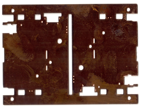
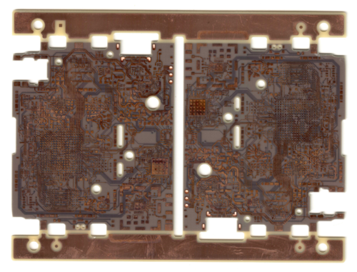
Now that both the laser and mechanical holes are drilled, Precursor’s PCB goes through a special step where the laser drilled vias are electroplated and filled to form functional and flat via-in-pad structures. Via-in-pad flatness is important to avoid assembly problems with the tiny WLCSP parts. At this point, the reddish oxide has been stripped off with an acid wash (which reduces the finished thickness very slightly, less than a micron), and the copper is once again shiny (even though this image doesn’t emphasize the reflective highlights so the vias are a bit easier to see). Excess plating is milled off the edges of the larger board’s cut-out features (such as the large gaps between the board panels), but the plating is left in-place on the smaller holes, even the non-plated ones.

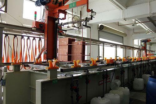
Above: an automated line used to plate copper onto PCBs.

Above: a view inside one of the many baths in the plating line.

Finally, Precursor’s PCB is taking a shape that we might recognize! Here, a “photoresist” layer has been added to define the outer traces. The astute observer will note the masked regions which are the regions of copper we want to *etch*, not the regions we want to *keep*. You’ll also note this “photoresist” is somehow able to cover large holes.
For the outer layers, it turns out that a “dry film” is used instead of an ink-like photoresist. One reason for this is we’re no longer dealing with a 2-D plane of copper: we have some plated-through holes we need to protect, and some non-plated holes we need to etch. A planar resist cannot adequately protect 3-D holes from etching. Thus, the board is covered with a conformal, photoreactive dry film capable of covering small holes. The dry film is exposed and developed to reveal the copper we wish to keep.
This brings us to the second reason for using the negative. At this point, additional copper is plated onto the unmasked copper regions to thicken the thin initial plating used to seed the mechanically drilled via holes, This simultaneously increases the finished thickness of the outer copper traces.
The masked and plated board is then dunked in a tin-plating bath that will fully cover all the exposed surfaces, including the 3-D structures of the plated-through vias we wish to keep. The tin plating can now serve as the etch mask. Next, the PCB is dunked into an etch vat to remove the photoresist and unwanted copper from not just the planar surfaces, but also from the vertical surfaces of the non-plated holes. Now etched, the PCB is finally stripped of the tin, leaving us once again with bare copper.

We’ve finally arrived at the near-finished six-layer, microvia PCB structure. At this point, all the electrically relevant structures have been built, so we just need to worry about the surface finishes.

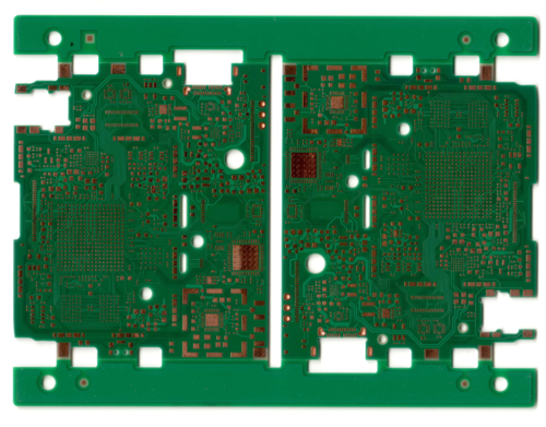
A protective layer of green soldermask is applied over the PCB. The soldermask is a photosensitive ink that is exposed in a process very similar to the photoresist process. Therefore it can image the very fine structures necessary to surround the tiny 0.4mm-pitch BGA structures used in Precursor. Almost any color of soldermask can be used, but green is the most common. At this point, small gaps in the soldermask are also imaged to assist with aligning the future v-scoring step.

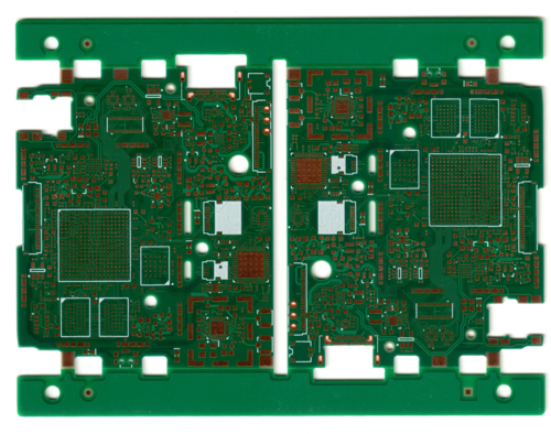
Next, a white silkscreen layer is applied. The silkscreen is mostly for human operators later in the process to know where components go. Normally, each component would have a “designator” attached to its location, but because we’re using predominantly 0201-sized components (a bit larger than a grain of salt), such designators would be illegible and not very useful. Instead, we pay a fairly hefty set-up fee for the SMT machine operator to go through a full manual check of the machine programming before assembly. Note that at this point, the pads are still bare copper and subject to oxidation if left exposed to air for a long time.

Above is the finished Precursor board, after the final two steps have been run: immersion gold plating and v-scoring. The immersion gold process deposits a very thin layer of gold over the exposed copper pads, protecting it from the elements. We use this instead of “HASL” (hot air levelled solder) because HASL is unable to achieve the planarity required for our small component geometries. “V-scoring” is the process of cutting V-shaped notches into the surface of a PCB to facilitate breaking off the sacrificial rails on the top and bottom (necessary for automated handling during the SMT process). You can see the subtle horizontal notches from the V-score in the image above.
Now finished, the board goes through an electrical test where every combination of pads is individually tested using a “flying probe” tester. These testers consist of several pairs of probes that can check the continuity of up to a hundred traces per second. On a complex board like Precursor’s, this test can take several minutes per board and is a significant driver of cost, After crowdfunding, some of the proceeds will be used to produce a “clamshell” type of test fixture with a bed-of-nails style tester to check all the circuit connections in a single mechanical operation.
After testing, the boards are packaged and sent to the SMT shop for assembly. And that’s how microvia PCBs are made! Precursor’s design would be classified as one of the simplest microvia constructions; smartphones will have 10 or more layers in their construction. Still, we can see why this construction is more expensive than on a conventional multi-layer board, since every successive microvia layer pair the PCB has to run through requires a full laminate, drill, and etch process cycle. Despite the extra cost, microvia is essential for mobile gadgets. As consumers demand ever-shrinking sizes, mechanically drilled vias can no longer meet routing density requirements. In addition to being a quarter the size of a mechanically drilled via, the use of blind through-vias in a typical microvia stack means component placing on the top and bottom side is largely independent of each other — it’s a bit like getting two PCBs in the space of one. This combination of denser vias and top/bottom placement freedom translates to a greater than 4x improvement in functional density over a conventional multi-layer board. In other words, even if we could make Precursor cheaper by using a conventional multi-layer board, it would be about 4x its current volume (about twice as thick, and perhaps 50% wider and longer)!
Finally, for the security-minded reader, there are a few observations we can make about implants in PCBs, now that we understand the detais of its construction. Because a PCB is made from a laminated stack of materials, we can see how it is possible to laminate an implant into a mid-layer of a PCB. The main trick is making sure the laminated implant can survive the autoclave conditions of 20x atmospheric pressure and 175C for an hour. It’s not inconceivable for a silicon chip to survive this, as they must survive soldering and package overmolding processes anyways.
If I were to do a buried implant in a PCB, I would build the inner core layer with the wirebonding pattern for the implant chip. Then I’d laminate the next layer of FR-4 with a cavity (an opening) for the implant chip, using a low-flow prepreg to bond the layers together. I’d then do a selective gold deposition on the chip’s bonding pads and wirebond the implant chip directly into the cavity. Note that chips are routinely thinned to less than 0.1mm in thickness, so the height of the chip is similar to that of the PCB laminate material. After bonding, I’d then encapsulate the implant chip in an epoxy (similar to the Epotek 301 resin shipped with Precursor for security sealing) to protect the wirebonds, then polish back any excess epoxy material so there is a smooth, void-free surface. At this point, I’d do a quick functional check of the implant before proceeding to the final FR-4 lamination steps, which would, as noted previously, obscure the implant’s presence from visual inspection.
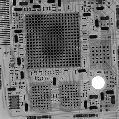
I estimate such a process could be developed in a matter of months (assuming non-pandemic times when travel to the factory was possible) for a few thousand dollars of material and process cost, assuming the implant chips were already available in a pre-thinned, known good die form. Thus, I’d say it’s neither hard nor inconceivable that one could bury an implant in a PCB; you don’t need to be a spy agency with a billion dollar budget to pull it off. However, detection of the implant is also pretty easy, as the chip would readily show up in any X-ray scan. Alternatively, an IR imager would likely pick up its presence, as the region of the implant would have a differential thermal conductivity and the implant itself may give off heat. Finally, if the chip isn’t carefully placed between two contiguous power planes, it could be picked out by simply shining light through the board. Thus, while it’s on the easier end of implants to execute, it’s also on the easier end of implants to detect.

Above is an x-ray view of an assembled Precursor PCB. A buried implant in the PCB would show up quite readily in such a scan, as you would see both modifications to the design’s trace pattern as well as the implant’s bond wires quite clearly in an x-ray. Note that x-ray scans like this are routine for quality management purposes during the manufacture of high-end electronic products.
If you want to learn more about Precursor, check out our crowdfunding page. Pre-orders help ensure that we can amortize all the setup costs of building our microvia PCBs. Even if Precursor isn’t the gadget for you, if you enjoyed this article, please consider leaving a donation by participating in the “buy us a couple of beers!” pledge tier.

