Winner, Name that Ware January 2020

February 29th, 2020

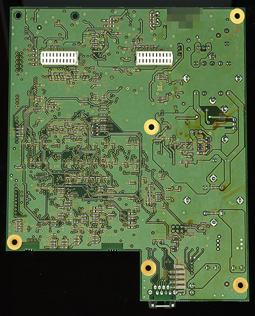
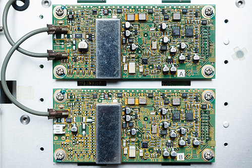
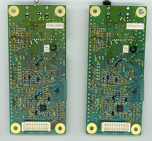
The ware for January 2020 is the brains of an IQ Motion Control position module. Congrats to Cody for guessing it, email me for your prize! And yes, I did blog about the modules a couple years ago, and since then I’ve found them to be an indispensable element of my mechatronic design toolbox. I’m just finishing up on delivering another successful design using these, so I had a couple extra laying about to take apart. If you’re doing any kind of motion control or robotics, it’s worth checking them out.

Name that Ware, January 2020

January 31st, 2020

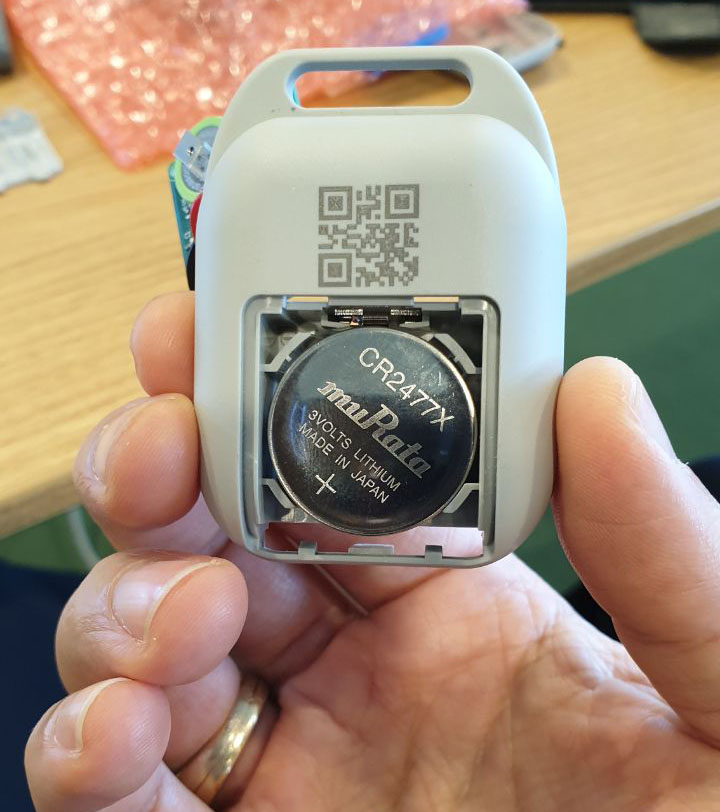
Welcome to a new year of name that ware! The first ware for 2020 is shown below.

There’s some aggressive image cropping going on to make it a little harder to guess, but there’s still plenty of hints laying around…

Winner, Name that Ware December

January 31st, 2020

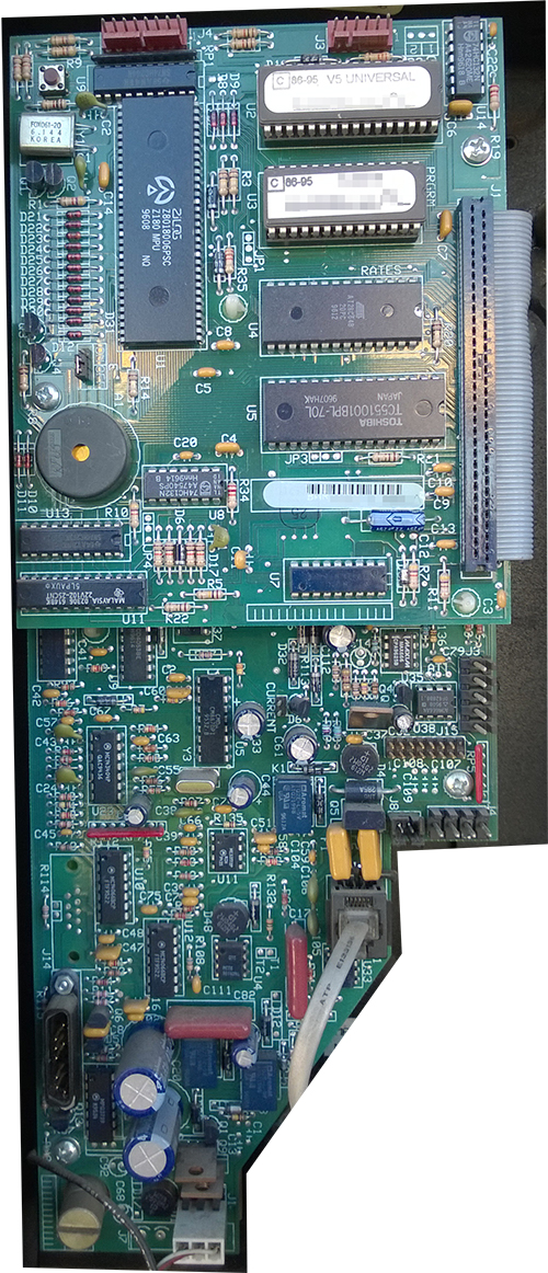
The ware for Dec 2019 is an async mux module from a PDP-11, more specifically, a DVZ11 quad asynchronous multiplexer (M7957). I found this board while rummaging among my childhood possessions looking for unrelated gear…I seem to recall picking it out of a trash pile at a local university back in the day. I had no idea what it was back then, it just looked cool. Congrats to dwu for naming it right away, email me for your prize!

Formlabs Form 3 Teardown

January 7th, 2020

It’s been my privilege to do teardowns on both the Formlabs Form 1 and Form 2. With the recent release of the Form 3, I was asked by Formlabs if I wanted to do another teardown, and of course I jumped on the opportunity. I always learn an immense amount while taking apart their machines, and it’s also been very satisfying to watch their engineering team grow and mature over the years.

Form 3 First Impressions

My first impression of the Form 3 was, “wow, this is a big machine”.

Above is a Form 3 next to a Form 1 for size comparison. The Form 3 build platform is a little larger than the Form 1, but it turns out there are a number of good reasons for the extra size, which we’ll get into later.

Before taking the whole machine apart, I decided I’d give it at least one test print. So, I went and downloaded a couple of popular-looking prints from the Internet and loaded them into the latest version of the Preform software. The design I had chosen was quite large, requiring over 18 hours to print in clear resin. This was not going to cut it for a quick test print! Fortunately, Formlabs had also sent me a sample of their “draft resin”, which advertises itself as a way to rough out quick, low-resolution prints. Indeed, migrating the design to the draft resin reduced the print time down to under 4 hours, which was a welcome relief for a quick test print.

The resin still yielded a part with reasonably crisp lines, although as expected the layers were quite visible. The main downside was that the part as printed was virtually impossible to remove from its support material. I suspect this might have been a user error, because I had changed the resin from clear to draft: I thought I had asked Preform to recompute the support material structure, but it seems that didn’t happen.

Above: a view of the test part, printed in draft resin.

Above: close-up of the rather robust support material connection to the print.

Aside from woes trying to remove the part from the support material, the other issues I had with the draft resin is its strong smell, and its sensitivity to ambient light. Everyone in the office became quite aware that I was using the draft resin due to its strong odor, so once the print was finished I endeavored to bottle up as much of the resin as I could, thus limiting the nuisance odor to others in the office. However, as I was handling the resin, I could see the draft resin was quickly curing in the ambient light, so I had to work quickly and pour it back into the bottle as a thin crust of material formed. Its increased photosensitivity makes sense, given that it is tuned for fast printing and curing, but it does make it a bit trickier to handle.

Overall, I’d probably give the draft resin another try because the fast print times are appealing, but that’ll be for another day – on to the teardown!

Exterior Notes

Even without removing a single screw, there’s a couple of noteworthy observations to share about the Form 3’s construction. Let’s start with the front panel UI.

The Form 3 doubles down on the sleek, movie-set ready UI of the Form 2.

Above is an example screen from the Form 3’s integrated display. In addition to a graphical style that would be at home in Tony Stark’s lab, the image above shows off the enhanced introspection capabilities of the printer. The Form 3 is more aware of its accessories and environment than ever; for example, it now has the ability to report a missing build platform.

One problem that became immediately evident to me, however, was a lack of a way to put the Form 3 into standby. I searched through the UI for a soft-standby option, but couldn’t find it. Perhaps it’s there, but it’s just very well hidden. However, the lack of a “hard” button to turn the system on from standby is possibly indicative of a deliberate choice to eliminate standby as an option. For good print quality, it seems the resin must be pre-heated to 30C, a process that could take quite some time in facilities that are kept cold or not heated. By maintaining the resin temperature even when the printer is not in use, Formlabs can reduce the “first print of the day” time substantially. Fortunately, Formlabs came up with a clever way to recycle waste heat from the electronics to heat the resin; we’ll go into that in more detail later.

As an aside, ever since I got a smart power meter installed at home, I’ve been trying to eliminate ghost power in the household; by going through my home and systemically shutting down devices that were under-utilized or poorly designed, I’ve managed to cut my power bill by a third. So, I took one of my in-line meters and measured the Form 3’s idle power. It clocks in at around 25 watts, or about 18kWh/mo; in Singapore I pay about US$0.10/kWh, so that’s a $21.60/yr or about 2% of my overall electric bill. I’ve migrated servers and shut them down for less, so probably I’d opt to unplug my Form 3 when it’s not in use, especially since my office is always pretty warm and the heat-up time for the resin would be fairly short.

The other thing that set the Form 3 apart from its predecessors is that when I looked inside, there were no optics in sight. Where I had expected to be staring at a galvanometer or mirror assembly, there was nothing but an empty metal pan, a lead screw, and a rather-serious looking metal box on the right hand side. I knew at this point the Form 3 was no incremental improvement over the Form 2: it was a clean-sheet redesign of their printing architecture.

Above: A view into the Form 3 body while idle, revealing nothing but an empty metal box.

I had deliberately avoided exposing myself to any of the press materials on the Form 3 prior to doing the teardown, so that my initial impressions would not be biased. But later on, I came to learn that the serious-looking metal box on the right hand side is called the “Light Processing Unit”, or LPU.

Power cycling the Form 3 quickly revealed that the LPU moves left to right on the internal lead screw. I immediately liked this new design, because it means that you no longer fouled the optics if your build platform dripped while the resin tank was removed. It also meant that the optics were much better sealed and protected, which means that the Form 3 would be much more resistant to smog, fog, and dust than its predecessors.

Power cycling the Form 3 causes it to exercise all its actuators as part of a self test, which gives you a nice, unobstructed view of the LPU outside of its stowage position, as shown above. Here, you can see that clearly, the galvanometer scans only in one dimension now, and that the optics look quite well sealed and protected.

▶️

Click the play button to hear the LPU scan

Because the LPU scans in one dimension, and the time it takes for the LPU to complete a scan is variable, the Form 3 makes a sort of “music” when it runs. I recorded a clip of what the LPU sounds like. It has a distinctive whah-whah sound as the servos vary the speed of the LPU as it scans across the print area. At the very conclusion of the short clip, you can hear the high-pitched whine of the LPU doing a “carriage return” across the entire print area. By analyzing the frequency of the sound coming from the LPU, you can infer the rough range of the line scanning rate for the LPU. For the sample I was printing, I get peaks at 23 Hz, 53 Hz, 298 Hz, followed by the carriage-return whine at around 5.2kHz.

Removing the Outer Shell

Taking off the outer panels reveal fabrication methodologies and design techniques that are more aligned with automotive or aerospace design schools than consumer electronics.

For example, the outer body panels of the Form 3 are made from shaped aluminum sheets that share more in common with the fender of a car than a 3D printer. 1.7mm thick sheet stock is bent into a compound 3D curve using some kind of stamping process, based on the work lines visible on the interior. The sheet then has keyhole fasteners added through a welding process (based on the heat-scoring around the fasteners) and the whole assembly is finally powder-coated.


Above: one of the aluminum “fenders” of the Form 3

This feels overall like a part I’d expect to see on a car or airplane, not on a 3D printer. However, the robustness of the body panels is probably commensurate with the weight of the Form 3 – at 17.5kg or 38.5lbs, it needs some pretty tough body panels to maintain tolerance and shape through shipping and handling.

A bit more wrangling, and the outer clear plastic shells come off. It’s worth noting the sheer size of these parts. They look to be largely molded or cast in one go, with some details like edge flanges glued on as a post-process. Getting a casting to work at this size with this quality is no small trick. There’s no marking on the part to indicate if it’s polycarbonate or acrylic, so I broke off a small corner and burned it. Based on the smell and how it burned, I’m guessing the orange outer case parts are probably cast acrylic.

With a pair of magnets taped to the rear edges of the case to defeat the safety interlocks, I’m able to run the printer with the covers off. Overall, it looks like the printer should be pretty easy to service for basic repairs and calibration in this state. But of course, we must go further…

Front Bezel

The front bezel of the Form 3 is constructed of a 2mm-thick glass [originally I had thought acrylic] sheet that’s been painted on the inside to create the rectangular opening for the screen. This creates a facade for the printer that recalls the design aesthetic of high-end mobile phones. This clear/painted sheet is then bonded to an ABS superstructure, featuring a robust structural thickness of around 3mm. The 16:9 LCD plus captouch screen is bonded into the clear hole in the acrylic. I’m guessing the resolution of the panel is probably 720p but no more than 1080p, given that the Lontium LT8918 LVDS-to-MIPI repeater embedded in the display’s drive FPC tops out at 1080p/60.

The LCD, touchscreen, and backlight are integrated with the “Display-o-Matic” board, which is held in place using a bit of double-sided tape. Peeling the board off its mounting reveals a small surprise. There’s two apertures cut into the paint next to the screen, along with a 12-LGA footprint that’s not populated. The wiring and empty footprint on the board would be apropos to an ST Microelectronics VL53L0X (or VL53L1X) proximity sensor. This neat little part can detect 1-D gestures up to 4 meters out using time-of-flight laser ranging. I imagine this might have been a candidate for the missing “on/off” switch on the Form 3, but for whatever reason it didn’t make the final cut.

Above: the aperture for the VL53L0X proximity sensor and correspnding empty land patterns on the Display-o-Matic PCB.

Main Circuit Cluster

The main circuit cluster for the Form 3 is located in the rear right of the printer. After pulling off the case, a set of PCBs comprising the main SoC module and driver electronics is clearly visible. Also note the “roll bar” that spans the rear of the printer – a lot of thought went into maintaining the dimensional stiffness of a fairly massive printer that also had to survive the abuse of a delivery courier.

A pair of Molex 2.4/5GHz FPC antennae form a diversity pair for the wifi on the printer. This is a generally good “punt” on RF performance when you have the space to afford a remote antenna: rather than struggling to cram an antenna into a tiny spot, it’s a reasonable approach to simply use a long-ish cable and place freespace-optimized antennae far away from your ground planes, and just hope it all works out. I was expecting to find one antenna oriented horizontally, and the other vertically, to try and capture some polarization diversity, but RF is a complicated thing and maybe other case structures conspired to make two horizontal antennae the best combination for this design.

Next to the antennae was another surprise: the Ethernet and USB breakout. The I/O ports are located on a circuit board that mechanically “floats” relative to the main PCB. This probably a blend of design constraint plus concerns about how a circuit board might fare as the most rigid element bridging a flexible polymer case to a rigid steel core in a 17.5kg product that’s subject to drop-kicking by couriers.

That the I/O ports are on its own PCB isn’t so strange; it’s the construction of that PCB and connector that is remarkable.

The breakout board is a rigi-flex PCB. This is perhaps one of the most expensive ways I can imagine implementing this, without a ton of benefit. Usually rigi-flex PCBs are reserved for designs that are extremely space-constrained, such that one cannot afford the space of a connector. While the USB2.0 speeds at 480Mbps are fast (and the Gigabit ethernet is even slower at 4x250Mbps diff pairs), it’s not so fast that it requires a rigi-flex PCB for impedance control; in fact, the opposing side is just a regular FPC that snaps into a rather unremarkable FPC connector (there are more exotic variants that would be invoked if signal integrity was really an issue). The flex portion does look like they’ve embedded a special solid conductor material for the reference plane, but normally one would just build exactly that – a flex cable with a reference plane that otherwise goes into two plain old FPC connectors.

Perhaps for some bizarre reason they couldn’t meet compliance on the USB connection and instead of re-spinning all of the main electronics boards they bought margin by using a Cadillac solution in one portion of the signal chain. However, I think it’s more likely that they are contemplating a more extensive use of rigi-flex technology in future iterations, but because there are relatively few reliable suppliers for this type of PCB, they are using this throw-away board as a “walk before you run” approach to learn how to work with a new and potentially difficult technology.

Turning from the I/O connectors to the main board, we see that like the Form 2, the Form 3 splits the system into a System-on-Module (SOM) plugged into a larger breakout board. Given the clearly extensive R&D budget poured into developing the Form 3, I don’t think the SOM solution was chosen because they couldn’t afford to build their own module; in fact, the SOM does bear a Formlabs logo, and uses a silkscreen font consistent with Altium, the design tool used for all the other boards. Unlike their other boards, this PCB lacks the designer’s initials and a cute code name.

My best guess is that this is somewhere in between a full-custom Formlabs design and an off the shelf OEM module. The position of the components are quite similar to those found on the Compulab CL-SOM-AM57x module, so probably Formlabs either licensed the design or paid CompuLab to produce and qualify a custom version of the SOM exclusively for Formlabs. For a further discussion of the trade-offs of going SOM vs fully integrated into a single PCB, check out my prior teardown of the Form 2. The TL;DR is that it doesn’t make economic sense to combine the two into a single board because the fine trace widths and impedance control needed to route the DDR memory bus on the CPU is wasted on the much larger bulk of the control PCB, along with other ancillary benefits of being able to modularize and split up the rather complex supply chain behind building the SOM itself.

The control breakout board once again relies on an STM32 CPU to do the real-time servo control, and Trinamic motor drivers. Thus from the perspective of the drive electronics and CPU, the Form 3 represents an evolutionary upgrade from the Form 2. However, this is about the only aspect of the Form 3 that is evolutionary when compared to the Form 2.

A Shout-Out to the Power Supply

The power supply: so humble, yet so under-appreciated. Its deceptively simple purpose – turning gunky AC line voltage into a seemingly inexhaustable pool of electrons with a constant potential – belies its complexity and bedrock role in a system. I appreciate the incorporation of a compact, solid, 200W, 24V @ 8.33A power supply in the Form 3, made by a reputable manufacturer.

Measuring Resin

The Form 2 had no real way of knowing how much resin was left in a cartridge, and it also used this wild projected capacitive liquid level sensor for detecting the amount of resin in the tank. When I saw it, I thought “wow, this has got to be some black magic”.

The Form 3 moves away from using a capacitive sensor – which I imagine is pretty sensitive to stray fields, humidity, and the varying material properties of the resin itself – to a mechanical float inside the tank.

One end of the float sits in the resin pool, while the other swings a small piece of metal up and down. My initial thought is that this bit of metal would be a magnet of some sort whose field is picked up by a hall effect sensor, except this introduces the problem of putting calibrated magnets into the resin tray.

It turns out they didn’t use a magnet. Instead, this bit of metal is just a lump of conductive material, and the position of the metal is sensed using an LDC1612 “inductance-to-digital” converter. This chip features a 28(!) bit ADC which claims sub-micron position sensing and a potential range of greater than 20cm. I didn’t even know these were a thing, but for what they are looking to do, it’s definitely a good chip for the job. I imagine with this system, there should be little ambiguity about the level of resin in the tank regardless of the environmental or dielectric properties of the resin. Variations in density might change the position of the float, but I imagine the float is so much more bouyant than the resin, so this variable would be a very minor factor.

The LDC1612 and its companion spiral PCB traces sit on a small daughtercard adjacent to the resin tank.

While the LDC1612 lets the Form 3 know how much resin is in the tank, but it still doesn’t answer the question of how much resin is left in the cartridge. The Form 3’s resin cartridge format is identical to the Form 2 (down to the camelback-style “bitevalve” and shampoo-cap air vent), so it seems modifying the cartridge was out of question. Perhaps they could have gone for some sort of capacitive liquid-level sensing strip running down the length of the device, but as mentioned above, capacitive sensors are fussy and subject to all sorts of false readings, screening problems and interference.

The Form 3’s solution to this problem is to incorporate a load cell into the resin cartridge mounting that weighs the resin cartridge in real-time. That’s right, there is a miniature digital scale inside every Form 3!

This is what the underside of the “digital scale” looks like. The top metal plate is where the resin tank sits, and the load cell is the silvery metal bar with a pair of overlapping holes drilled out of it on the right. The load-bearing connection for the top metal plate is the left hand side of the load cell, while the right hand side of the load cell is solidly screwed into the bottom metal plate. You can squeeze the two plates and see the top plate deflect ever so slightly. Load cells are extremely sensitive; this is exactly the sensor used in most precision digital scales. Accuracy and repeatability down to 10’s of milligrams is pretty easy to achieve with a load cell, so I imagine this works quite nicely to measure the amount of resin left in the tank. Just be sure not to rest any objects on top of your resin cartridge, or else you’ll throw off the reading!

Heating the Resin

In addition to measuring the resin levels, the Form 3 also needs to heat it. It seems the resin works best at slightly above normal room temperature, around 30C; and unless you live in Singapore, you’re going to need something to heat up the resin. The Form 2 used a nifty PCB-turned-heater around the resin tank. The Form 3 abandons this and incorporates basically a hair dryer inside the printer to heat the resin.

The hairdryer – erm resin heater – exhausts through a set of louvers to the left of the printer’s spine. The air is heated by a 120W, 24V heating element. I imagine they may not run it at a full 120W, but I do have to wonder how much of the Form 3 power supply’s 200W rating is budgeted to this one part alone. The “hairdryer” draws air that is pre-heated by the internal electronics of the Form 3, which may explain why the printer lacks an on/off button: assuming they had a goal of keeping the resin warm at all times, shutting down the main electronics just to turn it on again and then burn a 100+ watts to heat up your resin in a hurry doesn’t make much sense and is a bad user experience. I do like the elegance of recycling the waste heat of the electronics for a functional purpose; it makes me feel a little less bad that there is no way to put the printer into an apparent sleep mode.

The LPU

Now it’s time to get into the main act! The Light Processing Unit, or LPU, is the new “engine” of the Form 3. It’s the solid looking metal box that parks on the right hand side of the Form 3 when it’s idle, and scans back and forth across the print area during printing.

The LPU is a huge departure from the architecture of the previous Form 1 and 2 printers. The original Form printers used two galvanometers in series to create a 2-D laser scanning pattern. The total moving mass in this architecture is quite small. The theory behind the galvo-only design was that by relying just on the mesoscopic mass of the galvanometers, you can scan a laser to arbitrary points on a build stage, without being constrained by the physics of moving a macroscopic object like a print head: with a mechanical bandwidth on the order of 10kHz, a laser dot’s position can be shifted in a fraction of a millisecond. This also cuts back on large, heavy stepper motors, yielding a more compact design, and in some ways probably made the overall printer more forgiving of mechanical tolerances. The alignment features for all the critical optics could be machined into a single block, and any optics-to-build-stage alignment could theoretically be calibrated and “computed out” post-assembly.

However, in practice, anyone who has watched a Form print using a clear resin has probably noticed that the laser scan pattern rarely took advantage of the ability to take arbitrary paths. Most of the time, it scans across the build platform, with a final, quick step that traces the outlines of every build slice.

So why change the design? Although galvanometers can be expensive, having done a couple tear-downs of them I’m of the belief their high price is mostly reflective of their modest volumes, and not any fundamental material cost. After all, every mechanical hard drive shipped contains a voice coil capable of exquisite positioning resolution, and they don’t cost thousands of dollars. So it’s probably not a cost issue.

Other downsides of the original galvo-only construction include the laser beam taking an increasingly eccentric oval shape the further it gets off-axis, causing print resolution to be non-uniform across the build platform, and the active optics area being equivalent to the entire area under the build platform, meaning that resin drips and dust on the glass can lead to printing defects. The LPU architecture should, presumably, solve this problem.

Probably the biggest hint as to why the change is the introduction of the Form 3L: it roughly doubles the size of the build platform, while maintaining throughput by slaving two LPU’s in parallel. While it may be possible to tile 2-D galvanometer setups to increase the build platform size without reducing throughput, it would require stitching together the respective light fields of multiple galvanometers, which may be subject to drift over time. However, with the LPU, you could in theory create an arbitrarily long build platform in one axis, and then plug in more LPUs in parallel to improve your printing speed. Because they are all connected to the same mechanical leadscrew, their tolerances should drift together, leading to a robust and repeatable parallel printing architecture. The LPU architecture is extremely attractive if your company has a long-term vision of making 3D printing a mass production-capable process: it gives you more knobs to turn to give customers willing to pay a lot up front to improve their build throughput and/or latency. One could even imagine doubling the width of the build area by placing a second, opposite lead screw and interdigitating the LPUs.

It’s also worth mentioning that the introduction of the LPU has lead to a significant redesign of the resin tank. Instead of a silicone-based “peel” system, they have gone to a compound material system that gives them a flexible membrane during the “pull” step between layers, and a rigid platform by tensioning a hefty clear plastic sheet during the “print” phase. My gut tells me that this new platform also gives them a scaling path to larger build volumes, but I don’t know enough about the physics of what happens at the interface of the resin and the build stage to know for sure the trade-offs there.

The LPU also incorporates a number of other improvements that I think will have a huge impact on the Form 3’s overall performance and reliability:

• Because the galvo only needs to scan in 1 dimension, they are able to use a parabolic mirror to correct for the angle of the beam relative to the build platform. In other words, they are able to maintain a perpendicular, circular beam spot regardless of the build platform location, eliminating the loss of resolution toward the edges that a 2-D scanning system would suffer.
• The entire LPU is environmentally sealed. My Form 1 printer definitely suffered from a build-up of tiny particulates on the mirrors, and I’m dreading the day I have to clean the optics on my Form 2. While in theory they could have sealed the galvanometers of the Form 2, there’s still the huge build mirror and platform window to deal with. The LPU now has a single optical surface that looks trivial to wipe down with a quality lens cloth.
• The LPU can be “parked” during shipping and maintenance. This means zero risk of resin dripping on sensitive optical surfaces.
• The LPU is a separate, value-add module from the rest of the printer, allowing Formlabs to invest more heavily in the development of a critical component. It also opens up the possibility that Formlabs could OEM the LPU to low-cost manufacturers, allowing them to create a price-differentiated line of printers with less risk to their flagship brand name, while retaining a huge amount of control over the ecosystem.

The main downsides of the LPU, I imagine, are its sheer size and mass, and what appears to be an extremely tight mechanical tolerance spec for the alignment of the LPU relative to the build platform, both of which drive the overall size and mass of the system, presumably also driving up costs. Also, if you’re thinking ahead to the “millions” volumes of printers, my gut says the LPU is going to have a higher cost floor than a 2D galvo system. When you get to the point where tooling and R&D is fully amortized, and production yields are “chasing 9’s” (e.g. 99.9…%), you’re now talking about cost in terms of sheer bulk and mass of materials. It’s also more difficult in general to get good tolerance on large assemblies than small ones, so overall the LPU looks like a bet on quality, build volume scalability, and faster print times, at the expense of the overall potential cost floor.

OK, enough yammering, let’s get hammering!

This is a view of the LPU as-mounted in the printer, from the inside of the printer. On the left, you can see the lead screw responsible for shuttling the LPU back and forth. Just next to that you can see an array of three large silver screws and one large black thumb screw, all mounted on a cantilever-type apparatus. These seem to be used to do a final, critical alignment step of the LPU, presumably to get it to be perfectly perpendicular once all mechanical tolerances are accounted for. On the right hand side, there’s a blue anodized latching mechanism. I’m not sure what it’s for – my Form 3 arrived in a special shipping case, but perhaps on consumer units it’s meant to secure the LPU during shipping, and/or it’s used to assist with servicing and alignment. In the middle-bottom, you can see the protective cover for the galvonometer assembly, and of course the cooling fan for the overall LPU is smack dab in the middle.

I had to struggle a bit to extract the LPU. Eventually I figured out that the bottom plate of the printer can be detached, giving easy access to the LPU and its attached linear carriage.

The inside view of the Form 3 from the bottom-up also reveals the details of the calibration standard placed near the LPU’s parking spot. The calibration standard looks like it covers the entire build area, and it looks like it contains sufficient information to correct for both X and Y offsets, and the reflective-vs-matte coating presumably helps to correct for laser amplitude drift due to laser aging as well. I was a little surprised that the second dot pattern wasn’t a vernier of the first to increase the effective spatial resolution of the calibration pattern, but presumably this is sufficient to do the job. You can also see the hefty 24V motor used to pull the tensioning film on the resin tank, and the texture of the plastic body betrays the fact that the polymer is glass-filled for improved rigidity under these heavy loads.

There seems to be no graceful way to pull the LPU out without also bringing its linear carriage along for the ride, so I took both parts out as a single block. It’s a pretty hefty piece, weighing in at 2.5kg (5.6lb) inclusive of the carriage. Fortunately, the bulk of the mass is supported by a circular bearing on a rail beneath the carriage, and the actual absolute rate of acceleration required for the block isn’t so high as it is intended to scan in a smooth motion across the build surface.

Above is the LPU plus its linear carriage, now freed of the body of the Form 3. The die cast aluminum case of the LPU is reminiscent of an automotive ECU; I wouldn’t be surprised if a tour through the factory producing these cases revealed car parts rolling down a parallel line to the Form 3’s LPU case.

Removing the black polypropylene protective cover reveals the electronics baked into the LPU. There’s an STM32F745 Cortex-M7 with FPU, hinting that perhaps the LPU does substantial real-time processing internally to condition signals. An SMSC 332x USB PHY indicates that the LPU presents itself to the host system as a high-speed USB device; this should greatly simplify software integration for systems that incorporate multiple, parallel LPUs.

Aside from a smattering of analog signal conditioning and motor drivers, the board is fairly bare; mass is presumably not a huge concern, otherwise I’d imagine much of the rather dense FR-4 material would have been optimized out. I also appreciated the bit of aerospace humor on the board: next to the flex connector going to the galvanometer are the words “ATTACH ORBITER HERE / NOTE: BLACK SIDE DOWN”. These are the words printed on the struts which attached the Space Shuttle to the Shuttle Carrier Aircraft – a bit of NASA humor from back in the day.

Removing the mechanical interface between the LPU and the resin tank reveals a set of 2×3 high-strength magnets mounted on rotating arms that are used to pull the resin stir bar inside the tank, along with a pair of MLX90393 3-axis hall-effect sensors providing feedback on the position of the magnets.

Pulling the electronics assembly out of the LPU housing is a bit of a trick. As noted previously, the optics assembly is fully-sealed. Extracting the optical unit for inspection thus required cutting through a foam tape seal between the exterior glass plate and the interior sterile environment.

Thus freed, we can see some detail on the cantilever mount for the LPU core optics module. Clearly, there is some concern about the tolerance of the LPU relative to chassis, with extra CNC post-processing applied to clean up any extra tolerances plus some sort of mechanism to trim out the last few microns of alignment. I haven’t seen anything quite like this before, but imagine this is a structure I would have learned about if I had formally studied mechanics in college.

Finally, we arrive at the optics engine of the LPU. Removing the outer cover reveals a handsome optics package. The parabolic mirror is centrally prominent; immediately above it is the heat-sinked laser. Beneath the parabolic mirror is the galvanometer. Light fires from the laser, into the galvanometer, reflecting off a flat mirror (looks like a clear piece of glass, but presumably coated to optimally reflect the near-UV laser wavelength) down onto the parabolic mirror, and from there out the exit aperture to the resin tank. The white patch in the mid-left is a “getter” that helps maintain the environment within the environmentally sealed optical unit should any small amounts of contaminant make their way in.

There’s an incredibly subtle detail in the LPU that really made me do a double-take. There is a PCB inside that is the “Laser Scattering Detector” assembly. It contains six photodiodes that are used in conjunction with the calibration standard to provide feedback on the laser. The PCB isn’t flat – it’s ever so slightly curved. I’ve provided a shot of the PCB in the above photo, and highlighted the area to look for on the right hand side, so you can compare it to that on the left. If you look carefully, the board actually bends slightly toward the viewer in this image.

I scratched my head on this a bit – getting a PCB to bend at such an accurate curvature isn’t something that can be done in the PCB manufacturing process easily. It turns out the trick is that the mounting bosses for the PCB are slightly canted, so that once screwed into the bosses the PCB takes the shape of the desired curve. This is a pretty clever trick! Which lead me to wonder why they went through such trouble to curve the PCB. The sensors themselves are pretty large-area; I don’t think the curvature was added to increase the efficiency of light collection. My best guess is that because the laser beam fires perpendicularly onto the calibration standard, the scattered light would come straight back onto the photodetectors, which themselves are perpendicular to the beam, and thus may reflect light back onto the calibration standard. Bending the PCB at a slight angle would mean that any residual light reflected off of the dector assembly would be reflected into the aluminum body of the LPU, thus reducing the self-reflection signal of the detector assembly.

Above is a detail shot showing the galvanometer, laser, and parabolic mirror assembly, with the scattering light detector PCB removed so that all these components are clearly in view.

Finally, we get to the galvanometer. The galvo retains many of the features of the Form 2’s – the quadrature-based sensing and notched shaft. The most obvious improvements are a much smaller light source, perhaps to better approximate a “point” light source, with less interference from a surrounding LED housing, and the incorporation of some amplification electronics on the PCB, presumably to reduce the effect of noise pick-up as the cables snake their way around the system.

Epilogue

Well, that’s it for the Form 3 teardown – from the exterior shell down to the lone galvanometer. I’ve had the privilege of court-side seats to observe the growth of Formlabs. There’s a saying along the lines of “the last 20% takes 80% of the effort”. Based on what I’ve seen of the Form series, that should be amended to “the last 20% takes 80% of the effort – and then you get to start on the product you meant to make in the first place”. It dovetails nicely into the observation that products don’t hit their stride until the third version (remember Windows 3.x?). From three grad students fresh out of the MIT Media Lab to a billion-dollar company, Formlabs and the Form series of printers have come a long way. I’d count myself as one of the bigger skeptics of 3D printing as a mass-production technology, but I hadn’t considered an approach like the LPU. I feel like the LPU embodies an audacious vision of the future of 3D printing that was not obvious to me as an observer about nine years ago. I’m excited to see where this all goes from here!

Can We Build Trustable Hardware?

December 27th, 2019

Why Open Hardware on Its Own Doesn’t Solve the Trust Problem

A few years ago, Sean ‘xobs’ Cross and I built an open-source laptop, Novena, from the circuit boards up, and shared our designs with the world. I’m a strong proponent of open hardware, because sharing knowledge is sharing power. One thing we didn’t anticipate was how much the press wanted to frame our open hardware adventure as a more trustable computer. If anything, the process of building Novena made me acutely aware of how little we could trust anything. As we vetted each part for openness and documentation, it became clear that you can’t boot any modern computer without several closed-source firmware blobs running between power-on and the first instruction of your code. Critics on the Internet suggested we should have built our own CPU and SSD if we really wanted to make something we could trust.

I chewed on that suggestion quite a bit. I used to be in the chip business, so the idea of building an open-source SoC from the ground-up wasn’t so crazy. However, the more I thought about it, the more I realized that this, too was short-sighted. In the process of making chips, I’ve also edited masks for chips; chips are surprisingly malleable, even post tape-out. I’ve also spent a decade wrangling supply chains, dealing with fakes, shoddy workmanship, undisclosed part substitutions – there are so many opportunities and motivations to swap out “good” chips for “bad” ones. Even if a factory could push out a perfectly vetted computer, you’ve got couriers, customs officials, and warehouse workers who can tamper the machine before it reaches the user. Finally, with today’s highly integrated e-commerce systems, injecting malicious hardware into the supply chain can be as easy as buying a product, tampering with it, packaging it into its original box and returning it to the seller so that it can be passed on to an unsuspecting victim.

If you want to learn more about tampering with hardware, check out my presentation at Bluehat.il 2019.

Based on these experiences, I’ve concluded that open hardware is precisely as trustworthy as closed hardware. Which is to say, I have no inherent reason to trust either at all. While open hardware has the opportunity to empower users to innovate and embody a more correct and transparent design intent than closed hardware, at the end of the day any hardware of sufficient complexity is not practical to verify, whether open or closed. Even if we published the complete mask set for a modern billion-transistor CPU, this “source code” is meaningless without a practical method to verify an equivalence between the mask set and the chip in your possession down to a near-atomic level without simultaneously destroying the CPU.

So why, then, is it that we feel we can trust open source software more than closed source software? After all, the Linux kernel is pushing over 25 million lines of code, and its list of contributors include corporations not typically associated with words like “privacy” or “trust”.

The key, it turns out, is that software has a mechanism for the near-perfect transfer of trust, allowing users to delegate the hard task of auditing programs to experts, and having that effort be translated to the user’s own copy of the program with mathematical precision. Thanks to this, we don’t have to worry about the “supply chain” for our programs; we don’t have to trust the cloud to trust our software.

Software developers manage source code using tools such as Git (above, cloud on left), which use Merkle trees to track changes. These hash trees link code to their development history, making it difficult to surreptitiously insert malicious code after it has been reviewed. Builds are then hashed and signed (above, key in the middle-top), and projects that support reproducible builds enable any third-party auditor to download, build, and confirm (above, green check marks) that the program a user is downloading matches the intent of the developers.

There’s a lot going on in the previous paragraph, but the key take-away is that the trust transfer mechanism in software relies on a thing called a “hash”. If you already know what a hash is, you can skip the next paragraph; otherwise read on.

A hash turns an arbitrarily large file into a much shorter set of symbols: for example, the file on the left is turned into “cat-mouse-panda-bear”. These symbols have two important properties: even the tiniest change in the original file leads to an enormous change in the shorter set of symbols; and knowledge of the shorter set of symbols tells you virtually nothing about the original file. It’s the first property that really matters for the transfer of trust: basically, a hash is a quick and reliable way to identify small changes in large sets of data. As an example, the file on the right has one digit changed — can you find it? — but the hash has dramatically changed into “peach-snake-pizza-cookie”.

Because computer source code is also just a string of 1’s and 0’s, we can also use hash functions on computer source code, too. This allows us to quickly spot changes in code bases. When multiple developers work together, every contribution gets hashed with the previous contribution’s hashes, creating a tree of hashes. Any attempt to rewrite a contribution after it’s been committed to the tree is going to change the hash of everything from that point forward.

This is why we don’t have to review every one of the 25+ million lines of source inside the Linux kernel individually – we can trust a team of experts to review the code and sleep well knowing that their knowledge and expertise can be transferred into the exact copy of the program running on our very own computers, thanks to the power of hashing.

Because hashes are easy to compute, programs can be verified right before they are run. This is known as closing the “Time-of-Check vs Time-of-Use” (TOCTOU) gap. The smaller the gap between when the program is checked versus when it is run, the less opportunity there is for malicious actors to tamper with the code.

Now consider the analogous picture for open source in the context of hardware, shown above. If it looks complicated, that’s because it is: there are a lot of hands that touch your hardware before it gets to you!

Git can ensure that the original design files haven’t been tampered with, and openness can help ensure that a “best effort” has been made to build and test a device that is trustworthy. However, there are still numerous actors in the supply chain that can tamper with the hardware, and there is no “hardware hash function” that enables us to draw an equivalence between the intent of the developer, and the exact instance of hardware in any user’s possession. The best we can do to check a modern silicon chip is to destructively digest and delayer it for inspection in a SEM, or employ a building-sized microscope to perform ptychographic imaging.

It’s like the Heisenberg Uncertainty Principle, but for hardware: you can’t simultaneously be sure of a computer’s construction without disturbing its function. In other words, for hardware the time of check is decoupled from the time of use, creating opportunities for tampering by malicious actors.

Of course, we entirely rely upon hardware to faithfully compute the hashes and signatures necessary for the perfect trust transfer of trust in software. Tamper with the hardware, and all of a sudden all these clever maths are for naught: a malicious piece of hardware could forge the results of a hash computation, thus allowing bad code to appear identical to good code.

Three Principles for Building Trustable Hardware

So where does this leave us? Do we throw up our hands in despair? Is there any solution to the hardware verification problem?

I’ve pondered this problem for many years, and distilled my thoughts into three core principles:

1. Complexity is the enemy of verification. Without tools like hashes, Merkel trees and digital signatures to transfer trust between developers and users, we are left in a situation where we are reduced to relying on our own two eyes to assess the correct construction of our hardware. Using tools and apps to automate verification merely shifts the trust problem, as one can only trust the result of a verification tool if the tool itself can be verified. Thus, there is an exponential spiral in the cost and difficulty to verify a piece of hardware the further we drift from relying on our innate human senses. Ideally, the hardware is either trivially verifiable by a non-technical user, or with the technical help of a “trustable” acquaintance, e.g. someone within two degrees of separation in the social network.

2. Verify entire systems, not just components. Verifying the CPU does little good when the keyboard and display contain backdoors. Thus, our perimeter of verification must extend from the point of user interface all the way down to the silicon that carries out the secret computations. While open source secure chip efforts such as Keystone and OpenTitan are laudable and valuable elements of a trustable hardware ecosystem, they are ultimately insufficient by themselves for protecting a user’s private matters.

3. Empower end-users to verify and seal their hardware. Delegating verification and key generation to a central authority leaves users exposed to a wide range of supply chain attacks. Therefore, end users require sufficient documentation to verify that their hardware is correctly constructed. Once verified and provisioned with keys, the hardware also needs to be sealed, so that users do not need to conduct an exhaustive re-verification every time the device happens to leave their immediate person. In general, the better the seal, the longer the device may be left unattended without risk of secret material being physically extracted.

Unfortunately, the first and second principles conspire against everything we have come to expect of electronics and computers today. Since their inception, computer makers have been in an arms race to pack more features and more complexity into ever smaller packages. As a result, it is practically impossible to verify modern hardware, whether open or closed source. Instead, if trustworthiness is the top priority, one must pick a limited set of functions, and design the minimum viable verifiable product around that.

The Simplicity of Betrusted

In order to ground the conversation in something concrete, we (Sean ‘xobs’ Cross, Tom Mable, and I) have started a project called “Betrusted” that aims to translate these principles into a practically verifiable, and thus trustable, device. In line with the first principle, we simplify the device by limiting its function to secure text and voice chat, second-factor authentication, and the storage of digital currency.

This means Betrusted can’t browse the web; it has no “app store”; it won’t hail rides for you; and it can’t help you navigate a city. However, it will be able to keep your private conversations private, give you a solid second factor for authentication, and perhaps provide a safe spot to store digital currency.

In line with the second principle, we have curated a set of peripherals for Betrusted that extend the perimeter of trust to the user’s eyes and fingertips. This sets Betrusted apart from open source chip-only secure enclave projects.

Verifiable I/O

For example, the input surface for Betrusted is a physical keyboard. Physical keyboards have the benefit of being made of nothing but switches and wires, and are thus trivial to verify.

Betrusted’s keyboard is designed to be pulled out and inspected by simply holding it up to a light, and we support different languages by allowing users to change out the keyboard membrane.

The output surface for Betrusted is a black and white LCD with a high pixel density of 200ppi, approaching the performance of ePaper or print media, and is likely sufficient for most text chat, authentication, and banking applications. This display’s on-glass circuits are entirely constructed of transistors large enough to be 100% inspected using a bright light and a USB microscope. Below is an example of what one region of the display looks like through such a microscope at 50x magnification.

The meta-point about the simplicity of this display’s construction is that there are few places to hide effective back doors. This display is more trustable not just because we can observe every transistor; more importantly, we probably don’t have to, as there just aren’t enough transistors available to mount an attack.

Contrast this to the more sophisticated color displays, which rely on a fleck of silicon with millions of transistors implementing a frame buffer and command interface, and this controller chip is closed-source. Even if such a chip were open, verification would require a destructive method involving delayering and a SEM. Thus, the inspectability and simplicity of the LCD used in Betrusted is fairly unique in the world of displays.

Verifiable CPU

The CPU is, of course, the most problematic piece. I’ve put some thought into methods for the non-destructive inspection of chips. While it may be possible, I estimate it would cost tens of millions of dollars and a couple years to execute a proof of concept system. Unfortunately, funding such an effort would entail chasing venture capital, which would probably lead to a solution that’s closed-source. While this may be an opportunity to get rich selling services and licensing patented technology to governments and corporations, I am concerned that it may not effectively empower everyday people.

The TL;DR is that the near-term compromise solution is to use an FPGA. We rely on logic placement randomization to mitigate the threat of fixed silicon backdoors, and we rely on bitstream introspection to facilitate trust transfer from designers to user. If you don’t care about the technical details, skip to the next section.

The FPGA we plan to use for Betrusted’s CPU is the Spartan-7 FPGA from Xilinx’s “7-Series”, because its -1L model bests the Lattice ECP5 FPGA by a factor of 2-4x in power consumption. This is the difference between an “all-day” battery life for the Betrusted device, versus a “dead by noon” scenario. The downside of this approach is that the Spartan-7 FPGA is a closed source piece of silicon that currently relies on a proprietary compiler. However, there have been some compelling developments that help mitigate the threat of malicious implants or modifications within the silicon or FPGA toolchain. These are:

• The Symbiflow project is developing a F/OSS toolchain for 7-Series FPGA development, which may eventually eliminate any dependence upon opaque vendor toolchains to compile code for the devices.
Prjxray is documenting the bitstream format for 7-Series FPGAs. The results of this work-in-progress indicate that even if we can’t understand exactly what every bit does, we can at least detect novel features being activated. That is, the activation of a previously undisclosed back door or feature of the FPGA would not go unnoticed.
• The placement of logic with an FPGA can be trivially randomized by incorporating a random seed in the source code. This means it is not practically useful for an adversary to backdoor a few logic cells within an FPGA. A broadly effective silicon-level attack on an FPGA would lead to gross size changes in the silicon die that can be readily quantified non-destructively through X-rays. The efficacy of this mitigation is analogous to ASLR: it’s not bulletproof, but it’s cheap to execute with a significant payout in complicating potential attacks.

The ability to inspect compiled bitstreams in particular brings the CPU problem back to a software-like situation, where we can effectively transfer elements of trust from designers to the hardware level using mathematical tools. Thus, while detailed verification of an FPGA’s construction at the transistor-level is impractical (but still probably easier than a general-purpose CPU due to its regular structure), the combination of the FPGA’s non-determinism in logic and routing placement, new tools that will enable bitstream inspection, and the prospect of 100% F/OSS solutions to compile designs significantly raises the bar for trust transfer and verification of an FPGA-based CPU.


Above: a highlighted signal within an FPGA design tool, illustrating the notion that design intent can be correlated to hardware blocks within an FPGA.

One may argue that in fact, FPGAs may be the gold standard for verifiable and trustworthy hardware until a viable non-destructive method is developed for the verification of custom silicon. After all, even if the mask-level design for a chip is open sourced, how is one to divine that the chip in their possession faithfully implements every design feature?

The system described so far touches upon the first principle of simplicity, and the second principle of UI-to-silicon verification. It turns out that the 7-Series FPGA may also be able to meet the third principle, user-sealing of devices after inspection and acceptance.

Sealing Secrets within Betrusted

Transparency is great for verification, but users also need to be able to seal the hardware to protect their secrets. In an ideal work flow, users would:

1. Receive a Betrusted device

2. Confirm its correct construction through a combination of visual inspection and FPGA bitstream randomization and introspection, and

3. Provision their Betrusted device with secret keys and seal it.

Ideally, the keys are generated entirely within the Betrusted device itself, and once sealed it should be “difficult” for an adversary with direct physical possession of the device to extract or tamper with these keys.

We believe key generation and self-sealing should be achievable with a 7-series Xilinx device. This is made possible in part by leveraging the bitstream encryption features built into the FPGA hardware by Xilinx. At the time of writing, we are fairly close to understanding enough of the encryption formats and fuse burning mechanisms to provide a fully self-hosted, F/OSS solution for key generation and sealing.

As for how good the seal is, the answer is a bit technical. The TL;DR is that it should not be possible for someone to borrow a Betrusted device for a few hours and extract the keys, and any attempt to do so should leave the hardware permanently altered in obvious ways. The more nuanced answer is that the 7-series devices from Xilinx are quite popular, and have received extensive scrutiny over its lifetime by the broader security community. The best known attacks against the 256-bit CBC AES + SHA-256 HMAC used in these devices leverages hardware side channels to leak information between AES rounds. This attack requires unfettered access to the hardware and about 24 hours to collect data from 1.6 million chosen ciphertexts. While improvement is desirable, keep in mind that a decap-and-image operation to extract keys via physical inspection using a FIB takes around the same amount of time to execute. In other words, the absolute limit on how much one can protect secrets within hardware is probably driven more by physical tamper resistance measures than strictly cryptographic measures.

Furthermore, now that the principle of the side-channel attack has been disclosed, we can apply simple mitigations to frustrate this attack, such as gluing shut or removing the external configuration and debug interfaces necessary to present chosen ciphertexts to the FPGA. Users can also opt to use volatile SRAM-based encryption keys, which are immediately lost upon interruption of battery power, making attempts to remove the FPGA or modify the circuit board significantly riskier. This of course comes at the expense of accidental loss of the key should backup power be interrupted.

At the very least, with a 7-series device, a user will be well-aware that their device has been physically compromised, which is a good start; and in a limiting sense, all you can ever hope for from a tamper-protection standpoint.

You can learn more about the Betrusted project at our github page, https://betrusted.io. We think of Betrusted as more of a “hardware/software distro”, rather than as a product per se. We expect that it will be forked to fit the various specific needs and user scenarios of our diverse digital ecosystem. Whether or not we make completed Betrusted reference devices for sale will depend upon the feedback of the community; we’ve received widely varying opinions on the real demand for a device like this.

Trusting Betrusted vs Using Betrusted

I personally regard Betrusted as more of an evolution toward — rather than an end to — the quest for verifiable, trustworthy hardware. I’ve struggled for years to distill the reasons why openness is insufficient to solve trust problems in hardware into a succinct set of principles. I’m also sure these principles will continue to evolve as we develop a better and more sophisticated understanding of the use cases, their threat models, and the tools available to address them.

My personal motivation for Betrusted was to have private conversations with my non-technical friends. So, another huge hurdle in all of this will of course be user acceptance: would you ever care enough to take the time to verify your hardware? Verifying hardware takes effort, iPhones are just so convenient, Apple has a pretty compelling privacy pitch…and “anyways, good people like me have nothing to hide…right?” Perhaps our quixotic attempt to build a truly verifiable, trustworthy communications device may be received by everyday users as nothing more than a quirky curio.

Even so, I hope that by at least starting the conversation about the problem and spelling it out in concrete terms, we’re laying the framework for others to move the goal posts toward a safer, more private, and more trustworthy digital future.

The Betrusted team would like to extend a special thanks to the NLnet foundation for sponsoring our efforts.