I’ve often said that there are no secrets in hardware — you just need a bigger, better microscope.
I think I’ve found the limit to that statement. To give you an idea, here’s the “lightbulb” that powers the microscope:

It’s the size of a building, and it’s the Swiss Light Source. Actually, not all of that building is dedicated to this microscope, just one beamline of an X-ray synchrotron capable of producing photons at an energy of 6.5keV (X-rays) at a flux of close to a billion coherent photons per second — but still, it’s a big light bulb. It might be a while before you see one of these popping up in a hacker’s garage…err, hangar…somewhere.
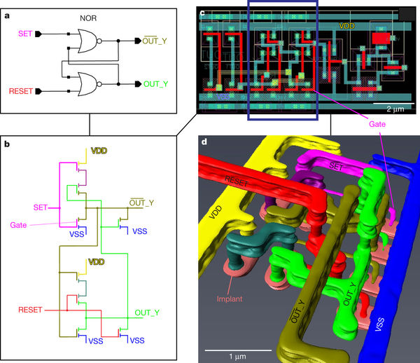
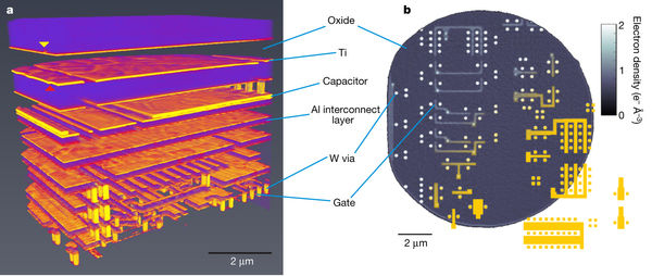
The result? One can image, in 3-D and “non-destructively” (e.g., without having to delayer or etch away dielectrics), chips down to a resolution of 14.6nm.


That’s a pretty neat trick if you’re trying to reverse engineer modern silicon.
You can read the full article at Nature (“High Resolution non-destructive three-dimensional imaging of integrated circuits” by Mirko Holler et al). I’m a paying subscriber to Nature so I’m supposed to have access to the article, but at the moment, their paywall is throwing a null pointer exception. Once the paywall is fixed you can buy a copy of the article to read, but in the meantime, SciHub seems more reliable.
You get what you pay for, right?
