I don’t do many teardowns on this blog, as several other websites already do an excellent job of that, but when I was given the chance to take apart a Formlabs Form 2, I was more than happy to oblige. About three yeargalvos ago, I had posted a teardown of a Form 1, which I received as a Kickstarter backer reward. Today, I’m looking at a Form 2 engineering prototype. Now that the Form 2 is in full production, the prototypes are basically spare parts, so I’m going to unleash my inner child and tear this thing apart with no concern about putting it back together again.
For regular readers of this blog, this teardown takes the place of March 2016’s Name that Ware — this time, I’m the one playing Name that Ware and y’all get to follow along as I adventure through the printer. Next month I’ll resume regular Name that Ware content.
First Impressions

I gave the Form 2 a whirl before tearing it into an irreparable pile of spare parts. In short, I’m impressed; the Form 2 is a major upgrade from the Form 1. It’s an interesting contrast to Makerbot. The guts of the Makerbot Replicator 2 are basically the same architecture as previous models, inheriting all the limitations of its previous incarnation.
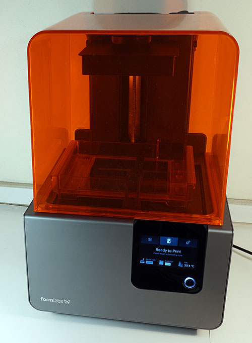
The Form 2 is a quantum leap forward. The product smells of experienced, seasoned engineers; a throwback to the golden days of Massachusetts Route 128 when DEC, Sun, Polaroid and Wang Laboratories cranked out quality American-designed gear. Formlabs wasn’t afraid to completely rethink, re-architect, and re-engineer the system to build a better product, making bold improvements to core technology. As a result, the most significant commonality between the Form 1 and the Form 2 is the iconic industrial design: an orange acrylic box sitting atop an aluminum base with rounded corners and a fancy edge-lit power button.
Before we slip off the cover, here’s a brief summary of the upgrades that I picked up on while doing the teardown:
The CPU is upgraded from a single 72MHz ST Micro STM32F103 Cortex-M3 to a 600 MHz TI Sitara AM3354 Cortex A8, with two co-processors: a STM32F030 as a signal interface processor, and a STM32F373 as a real-time DSP on the galvo driver board.
This massive upgrade in CPU power leapfrogs the UI from a single push button plus monochrome OLED on the Form 1, to a full-color 4.3” capacitive touch screen on the Form 2.
The upgraded CPU also enables the printer to have built-in wifi & ethernet, in addition to USB. Formlabs thoughtfully combines this new TCP/IP capability with a Bonjour client. Now, computers can automatically discover and enumerate Form 2’s on the local network, making setup a snap.
The UI also makes better use of the 4 GB of on-board FLASH by adding the ability to “replay” jobs that were previously uploaded, making the printer more suitable for low volume production.
The galvanometers are full custom, soup-to-nuts. We’ll dig into this more later, but presumably this means better accuracy, better print jobs, and a proprietary advantage that makes it much harder for cloners to copy the Form 2.
The optics pathway is fully shrouded, eliminating dust buildup problems. A beautiful and much easier to clean AR-coated glass surface protects the internal optics; internal shrouds also limit the opportunity for dust to settle on critical surfaces.
The resin tray now features a heater with closed-loop control, for more consistent printing performance in cold New England garages in the dead of winter.
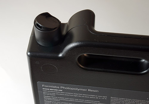
The resin tray is now auto-filling from an easy to install cartridge, enabling print jobs that require more resin than could fit in a single tank while making resin top-ups convenient and spill-free.
The peel motion is now principally lateral, instead of vertical.
The resin tank now features a stirrer. On the Form 1, light scattering would create thickened pools of partially cured resin near the active print region. Presumably the stirrer helps homogenize the resin; I also remember someone once mentioning the importance of oxygen to the surface chemistry of the resin tank.
There are novel internal photosensor elements that hint at some sort of calibration/skew correction mechanism
There’s a tilt sensor and manual mechanical leveling mechanism. A level tank prevents the resin from pooling to one side.
There are sensors that can detect the presence of the resin tank and the level of the resin. With all these new sensors, the only way a user can bork a print is to forget to install the build platform
Speaking of tank detection, the printer now remembers what color resin was used on a given tank, so you don’t accidentally spoil a clear resin tank with black resin
The power supply is now fully embedded; goodbye PSU failures and weird ground loop issues. It’s a subtle detail, but it’s the sort of “grown-up” thing that younger companies avoid doing because it complicates safety certification and requires compliance to elevated internal wiring and plastic flame retardance standards.
I’m also guessing there are a number of upgrades that are less obvious from a visual inspection, such as improvements to the laser itself, or optimizations to the printing algorithm.
These improvements indicate a significant manpower investment on the part of Formlabs, and an incredible value add to the core product, as many of the items I note above would take several man-months to bring to production-ready status.
Test Print

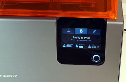
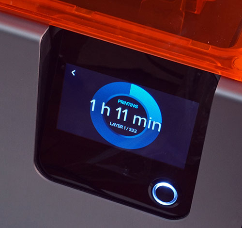
As hinted from the upgrade list, the UI has been massively improved. The touchscreen-based UI features tech-noir themed iconography and animations that would find itself at home in a movie set. This refreshing attention to detail sets the Form 2’s UI apart from the utilitarian “designed-by-programmers-for-geeks” UI typical of most digital fabrication tools.

A UI that would seem at home on a Hollywood set. Life imitating art imitating life.
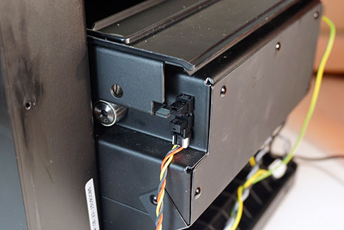
Unfortunately, the test print didn’t go smoothly. Apparently the engineering prototype had a small design problem which caused the resin tray’s identification contacts to intermittently short against the metal case during a peel operation. This would cause the bus shared between the ID chips on the resin tank and the filler cartridge to fail. As a result, the printer paused twice on account of a bogus “missing resin cartridge” error. Thankfully, the problem would eventually fix itself, and the print would automatically resume.

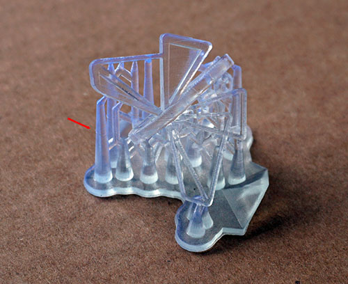
Test print from the Form 2. The red arrow indicates the location of a hairline artifact from the print pausing for a half hour due to issues with resin cartridge presence detection.
The test print came out quite nicely, despite the long pauses in printing. There’s only a slight, hairline artifact where the printer had stopped, so that’s good – if the printer actually does run out of resin, the printer can in fact pause without a major impact on print quality.
Significantly, this problem is fixed in my production unit – with this unit, I’ve had no problems with prints pausing due to the resin cartridge ID issue. It looks like they tweaked the design of the sheet metal around the ID contacts, giving it a bit more clearance and effectively solving the problem. It goes to show how much time and resources are required to vet a product as complex as a 3D printer – with so many sensors, moving parts, and different submodules that have to fit together perfectly throughout a service life involving a million cycles of movement, it takes a lot of discipline to chase down every last detail. So far, my production Form 2 is living up to expectations.
Removing the Outer Shell
I love that the Form 2, like the Form 1, uses exclusively hex and torx drive fasteners. No crappy philips or slotted screws here! They also make extensive use of socket cap style, which is a perennial favorite of mine.


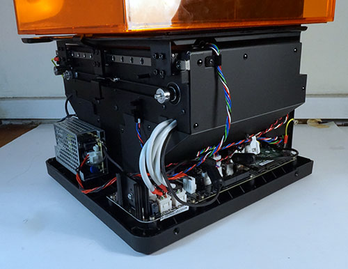
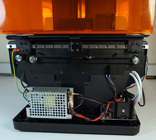
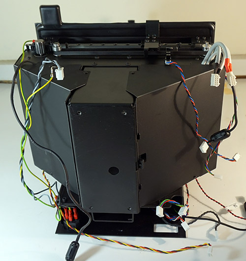
Removing the outer shell and taking a look around, we continue to see evidence of thoughtful engineering. The cable assemblies are all labeled and color-coded; there’s comprehensive detail on chassis grounding; the EMI countermeasures are largely designed-in, as opposed to band-aided at the last minute; and the mechanical engineering got kicked up a notch.

I appreciated the inclusion of an optical limit switch on the peel drive. The previous generation’s peel mechanism relied on a mechanical clutch with a bit of overdrive, which meant every peel cycle ended with a loud clicking sound. Now, it runs much more quietly, thanks to the feedback of the limit switch.

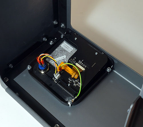
Backside of the Form 2 LCD + touchscreen assembly.
The touchpanel and display are mounted on the outer shell. The display is a DLC0430EZG 480×272 pixel TFT LCD employing a 24-bit RGB interface. I was a bit surprised at the use of a 30-pin ribbon cable to transmit video data between the electronics mainboard and the display assembly, as unshielded ribbon cables are notorious for unintentional RF emissions that complicate the certification process. However, a closer examination of the electronics around the ribbon cable reveal the inclusion of a CMOS-to-LVDS serdes IC on either side of the cable. Although this increases the BOM, the use of differential signaling greatly reduces the emissions footprint of the ribbon cable while improving signal integrity over an extended length of wire.
Significantly, the capacitive touchpanel’s glass seems to be a full custom job, as indicated by the fitted shape with hole for mounting the power button. The controller IC for the touchpanel is a Tango C44 by PIXCIR, a fabless semiconductor company based out of Suzhou, China. It’s heartening to see that the market for capacitve touchpanels has commoditized to the point where a custom panel makes sense for a relatively low volume product. I remember trying to source captouch solutions back in 2008, just a couple years after the iPhone’s debut popularized capacitive multi-touch sensors. It was hard to get any vendor to return your call if you didn’t have seven figures in your annual volume estimate, and the quoted NRE for custom glass was likewise prohibitive.

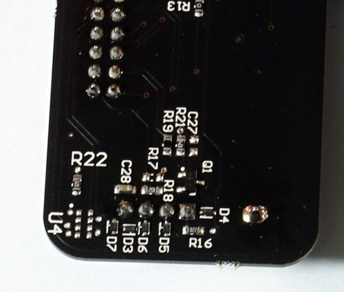
Before leaving the touchpanel and display subsection, I have to note with a slight chuckle the two reference designators (R22 and U4) that are larger than the rest. It’s a purely cosmetic mistake which I recognize because I’ve done it myself several times. From the look of the board, I’m guessing it was designed using Altium. Automatic ECOs in Altium introduce new parts with a goofy huge default designator size, and it’s easy to miss the difference. After all, you spend most of your time editing the PCB with the silkscreen layer turned off.
The Electronics
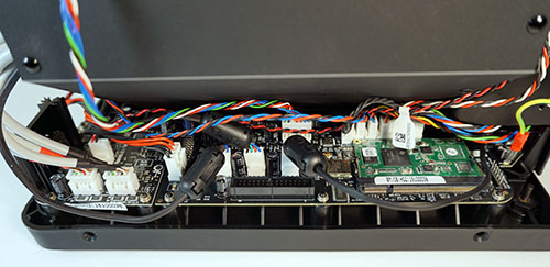
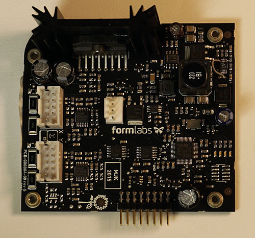
As an electronics geek, my attention was first drawn to the electronics mainboard and the galvanometer driver board. The two are co-mounted on the right hand side of the printer, with a single 2×8 0.1” header spanning the gap between the boards. The mounting seems to be designed for easy swapping of the galvanometer board.

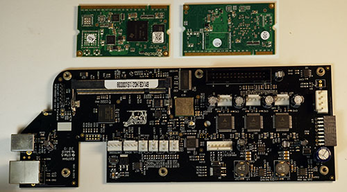
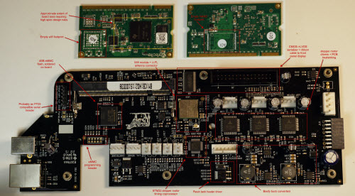
I have a great appreciation for Formlabs’ choice of using a Variscite SOM (system-on-module). I can speak from first-hand experience, having designed the Novena laptop, that it’s a pain in the ass to integrate a high speed CPU, DDR3 memory, and power management into a single board with complex mixed-signal circuitry. Dropping down a couple BGA’s and routing the DDR3 fly-by topology while managing impedance and length matching is just the beginning of a long series of headaches. You then get to look forward to power sequencing, hardware validation, software drivers, factory testing, yield management and a hundred extra parts in your supply chain. Furthermore, many of the parts involved in the CPU design benefit from economies of scale much larger than can be achieved from this one product alone.
Thus while it may seem attractive from a BOM standpoint to eliminate the middleman and integrate everything into a single PCB, from a system standpoint the effort may not amortize until the current version of the product has sold a few thousand units. By using a SOM, Formlabs reduces specialized engineering staff, saves months on the product schedule, and gains the option to upgrade their CPU without having to worry about amortization.
Furthermore, the pitch of the CPU and DDR3 BGAs are optimized for compact designs and assume a 6 or 8-layer PCB with 3 or 4-mil design rules. If you think about it, only the 2 square inches around the CPU and DRAM require these design rules. If the entire design is just a couple square inches, it’s no big deal to fab the entire board using premium design rules. However, the Form 2’s main electronics board is about 30 square inches. Only 2 square inches of this would require the high-spec design rules, meaning they would effectively be fabricating 28 square inches of stepper motor drivers using an 8-layer PCB with 3-mil design rules. The cost to fabricate such a large area of PCB adds up quickly, and by reducing the technology requirement of the larger PCB they probably make up decent ground on the cost overhead of the SOM.
Significantly, Formlabs was very selective about what they bought from Variscite: the SOM contained neither Wifi nor FLASH memory, even though the SOM itself had provisions for both. These two modules can be integrated onto the mainboard without driving up technology requirements, so Formlabs opted to self-source these components. In essence, they kept Variscite’s mark-up limited to a bare minimum set of components. The maturity to pick and choose cost battles is a hallmark of an engineering team with experience working in a startup environment. Engineers out of large, successful companies are used to working with virtually limitless development budgets and massive purchasing leverage, and typically show less discretion when allocating effort to cost reduction.

Mainboard assembly with SOM removed; back side of SOM is photoshopped into the image for reference.
I also like that Formlabs chose to use eMMC FLASH, instead of an SD card, for data storage. It’s probably a little more expensive, but the supply chain for eMMC is a bit more reliable than commodity SD memory. As eMMC is soldered onto the board, J3 was added to program the memory chip after assembly. It looks like the same wires going to the SOM are routed to J3, so the mainboard is probably programmed before the SOM is inserted.
Formlabs also integrates the stepper motor drivers into the mainboard, instead of using DIP modules like the Makerbot did until at least the Replicator’s Mighty Board Rev E. I think the argument I heard for the DIP modules was serviceability; however, I have to imagine the DIP modules are problematic for thermal management. PCBs are pretty good heatsinks, particularly those with embedded ground planes. Carving up the PCB into tiny modules appreciably increases the thermal resistance between the stepper motor driver and the air around it, which might actually drive up the failure rate. The layout of the stepper motor drivers on the Formlabs mainboard show ample provisions for heat to escape the chips into the PCB through multiple vias and large copper fills.

Mainboard assembly with annotations according to the discussion in this post.
Overall, the mainboard was thoughtfully designed and laid out; the engineering team (or engineer) was thinking at a system-level. They managed to escape the “second system effect” by restrained prioritization of engineering effort; just because they raised a pile of money didn’t mean they had to go re-engineer all the things. I also like that the entire layout is single-sided, which simplifies assembly, inspection and testing.
I learned a lot from reading this board. I’ve often said that reading PCBs is better than reading a textbook for learning electronics design, which is part of the reason I do a monthly Name that Ware. For example, I don’t have extensive experience in designing motor controllers, so next time I need to design a stepper motor driver, I’m probably going to have a look at this PCB for ideas and inspiration – a trivial visual inspection will inform me on what parts they used, the power architecture, trace widths, via counts, noise isolation measures and so forth. Even if the hardware isn’t Open, there’s still a lot that can be learned just by looking at the final design.

Now, I turn my attention to the galvanometer driver board. This is a truly exciting development! The previous generation used a fully analog driver architecture which I believe is based on an off-the-shelf galvanometer driver. A quick look around this PCB reveals that they’ve abandoned closing the loop in the analog domain, and stuck a microcontroller in the signal processing path. The signal processing is done by a STM32F373 – a 72 MHz, Cortex-M4 with FPU, HW division, and DSP extensions. Further enhancing its role as a signal processing element, the MCU integrates a triplet of 16-bit sigma-delta ADCs and 12-bit DACs. The board also has a smattering of neat-looking support components, such as a MCP42010 digital potentiometer, a fairly handsome OPA4376 precision rail-to-rail op amp, and a beefy LM1876 20W audio amplifier, presumably used to drive the galvanometer voice coils.
The power for the audio amplifier is derived from a pair of switching regulators, a TPS54336A handling the positive rail, and an LTC3704 handling the negative rail. There’s a small ECO wire on the LTC3704 which turns off burst mode operation; probably a good idea, as burst mode would greatly increase the noise on the negative rail, and in this application standby efficiency isn’t a paramount concern. I’m actually a little surprised they’re able to get the performance they need using switching regulators, but with a 20W load that may have been the only practical option. I guess the switching regulator’s frequency is also much higher than the bandwidth of the galvos, so maybe in practice the switching noise is irrelevant. There is evidence of a couple of tiny SOT-23 LDOs scattered around the PCB to clean up the supplies going to sensitive analog front-end circuitry, and there’s also this curious combination of a FQD7N10L NFET plus MPC6L02 dual op-amp. It looks like they intended the NFET to generate some heat, given the exposed solder slug on the back side, which makes me think this could be a discrete pass-FET LDO of some type. There’s one catch: the MCP6L02 can only operate at up to 6V, and power inside the Form 2 is distributed at 24V. There’s probably something clever going on here that I’m not gathering from a casual inspection of the PCBs; perhaps later I’ll break out some oscope probes to see what’s going on.
Overall, this ground-up redesign of the galvanometer driver should give Formlabs a strong technological foundation to implement tricks in the digital domain, which sets it apart from clones that still rely upon off-the-shelf fully analog galvanometer driver solutions.

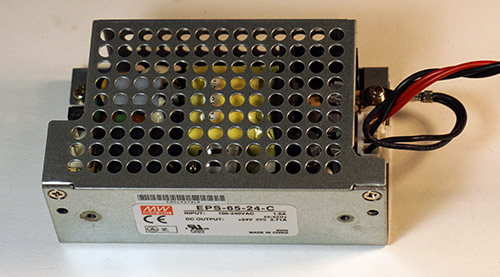
Before leaving our analysis of the electronics, let’s not forget the main power supply. It’s a Meanwell EPS-65-24-C. The power supply itself isn’t such a big deal, but the choice to include it within the chassis is interesting. Many, if not most, consumer electronic devices prefer to use external power bricks because it greatly simplifies certification. Devices that use voltages below 60V fall into the “easy” category for UL and CE certification. By pulling the power supply into the chassis, they are running line voltages up to 240V inside, which means they have to jump through IEC 60950-1 safety testing. It ups the ante on a number of things, including the internal wiring standards and the flame retardance of any plastics used in the assembly. I’m not sure why they decided to pull the power supply into the chassis; they aren’t using any fancy point-of-load voltage feedback to cancel out IR drops on the cable. My best guess is they felt it would either be a better customer experience to not have to deal with an external power brick, or perhaps they were bitten in the previous generation by flaky power bricks or ground loop/noise issues that sometimes plague devices that use external AC power supplies.
The Mechanical Platform
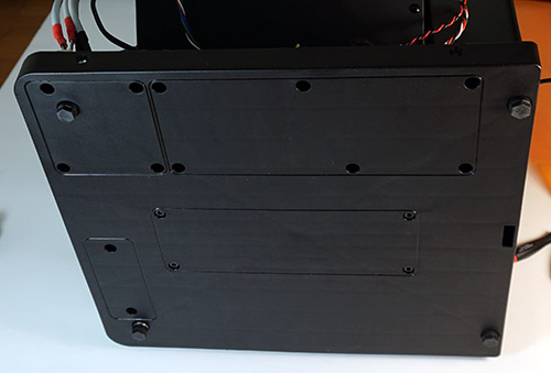
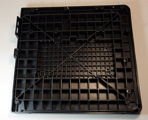
It turns out that my first instinct to rip out the electronics was probably the wrong order for taking apart the Form 2. A closer inspection of the base reveals a set of rounded rectangles that delineate the screws belonging to each physical subsystem within the device. This handy guide makes assembly (and repair) much easier.

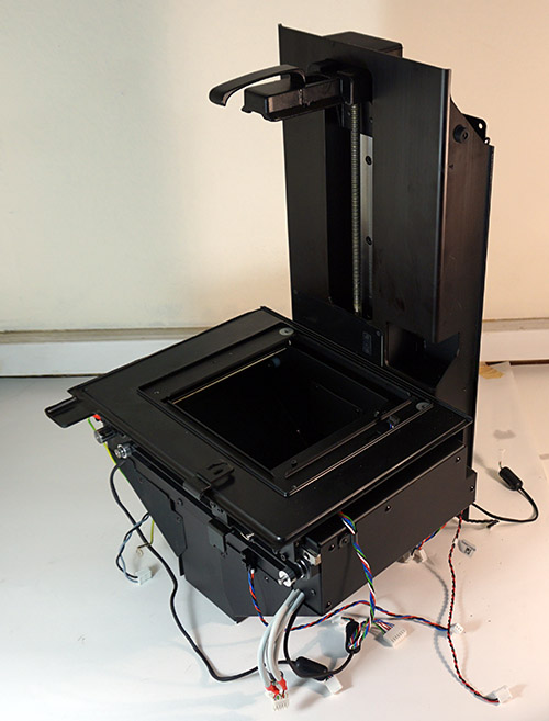
The central set of screws hold down the mechanical platform. Removing those causes the whole motor and optics assembly to pop off cleanly, giving unfettered access to all the electronics.

I’m oddly excited about the base of the Form 2. It looks like just a humble piece of injection molded plastic. But this is an injection molded piece of plastic designed to withstand the apocalypse. Extensive ribbing makes the base extremely rigid, and resistant to warpage. The base is also molded using glass-filled polymer – the same tough stuff used to make Pelican cases and automotive engine parts. I’ve had the hots for glass-filled polymers recently, and have been itching for an excuse to use it in one of my designs. Glass-filled polymer isn’t for happy-meal toys or shiny gadgets, it’s tough stuff for demanding applications, and it has an innately rugged texture. I’m guessing they went for a bomb-proof base because anything less rigid would lead to problems keeping the resin tank level. Either that, or someone in Formlabs has the same fetish I have for glass filled polymers.

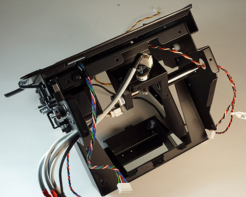
Once removed from the base, the central mechanical chassis stands upright on its own. Inside this assembly is the Z-axis leadscrew for the build platform, resin level sensor, resin heater, peel motor, resin stirrer, and the optics engine.

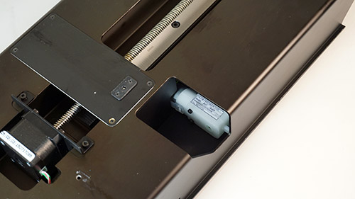
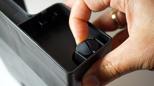
Here’s a close-up of the Z-stepper motor + leadscrew, resin level & temperature sensor, and resin valve actuator. The resin valve actuator is a Vigor Precision BO-7 DC motor with gearbox, used to drive a swinging arm loaded with a spring to provide the returning force. The arm pushes on the integral resin cartridge valve, which looks uncannily like the bite valve from a Camelback.

The resin tank valve is complimented by the resin tank’s air vent, which also looks uncannily like the top of a shampoo bottle.

My guess is Formlabs is either buying these items directly from the existing makers of Camelback and shampoo products, in which case First Sale Doctrine means any patent claims that may exist on these has been exhausted, or they have licensed the respective IP to make their own version of each.
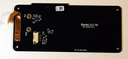
The resin level and temperature sensor assembly is also worth a closer look. It’s a PCB that’s mounted directly behind the resin tank, and in front of the Z-motor leadscrew.

Backside of the PCB mounted directly behind the resin tank.
It looks like resin level is measured using a TI FDC1004 capacitive liquid level sensor. I would have thought that capacitive sensing would be too fussy for accurate liquid level sensing, but after reading the datasheet for the FDC1004 I’m a little less skeptical. However, I imagine the sensor is extremely sensitive to all kinds of contamination, the least of which is resin splattered or dripped onto the sensor PCB.

Detail of the sensor PCB highlighting the non-contact thermopile temperature sensor.
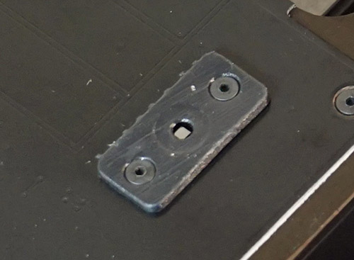
The resin temperature sense mechanism is also quite interesting. You’ll note a little silvery square, shrouded in plastic, mounted on the PCB behind the resin tank. First of all, the plastic shroud on my unit is clearly a 3D printed piece done by another Formlabs printer. You can see the nubs from the support structure and striation artifacts from the buildup process. I love that they’re dogfooding and using their own products to prototype and test; it’s a bad sign if the engineering team doesn’t believe in their own product enough to use it themselves.
Unscrewing the 3D printed shroud reveals a curious flip-chip CSP device, which I’m guessing is a TI TMP006 or TMP007 MEMS therompile. Although there are no part numbers on the chip, a quick read through the datasheet reveals a reference layout that is a dead ringer for the pattern on the PCB around the chip. Thermopiles can do non-contact remote temperature sensing, and it looks like this product has an accuracy of about +/-1 C between 0-60C. This explains the mystery of how they’re able to report the resin temperature on the UI without any sort of probe dipping into the resin tank.
But then how do they heat it? Look under the resin tank mount, and we find another PCB.

When I first saw this board, I thought its only purpose was to hold the leafspring contacts for the ID chip that helps track individual resin tanks and what color resin was used in them. Flip the PCB over, and you’ll see a curious pinkish tape covering the reverse surface.

The pinkish tape is actually a thermal gap sealer, and peeling the tape back reveals that the PCB itself has a serpentine trace throughout, which means they are using the resistivity of the copper trace on the PCB itself as a heating mechanism for the resin.

Again, I wouldn’t have guessed this is something that would work as well as it does, but there you have it. It’s a low-cost mechanism for controlling the temperature of the resin during printing. Probably the PCB material is the most expensive component, even more than the thermopile IR sensor, and all that’s needed to drive the heating element is a beefy BUK9277 NFET.
I’ve been to the Formlabs offices in Boston, and it does get rather chilly and dry there in the winter, so it makes sense they would consider cold temperature as a variable that could cause printing problems on the Form 2.
Cold weather isn’t a problem here in Singapore; however, persistent 90% humidity conditions is an issue. If I didn’t use my Form 1 for several weeks, the first print would always come out badly; usually I’d have to toss the resin in the tank and pour a fresh batch for the print to come out. I managed to solve this problem by placing a large pack of desiccant next to the resin tank, as well as using the shipping lid to try to seal out moisture. However, I’m guessing they have very few users in the tropics, so humidity-related print problems are probably going to be a unique edge case I’ll have to solve on my own for some time to come.
The Optics Pathway
Finally, the optics – I’m saving the best for last. The optics pathway is the beating heart of the Form 2.

The last thing uncured resin sees before it turns into plastic.
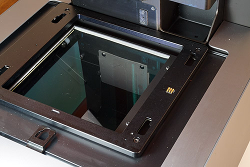
The first thing I noticed about the optics is the inclusion of a protective glass panel underneath the resin tank. In the Form 1, if the build platform happened to drip resin while the tank was removed, or if the room was dusty, you had the unenviable task of reaching into the printer to clean the mirror. The glass panel simplifies the cleaning operation while protecting sensitive optics from dust and dirt.

I love that the protective glass has an AR coating. You can tell there’s an AR coating from the greenish tint of the reflections off the surface of the glass. AR coatings are sexy; if I had a singles profile, you’d see “the green glint of AR-coated glasses” under turn-ons. Of course, the coating is there for functional reasons – any loss of effective laser power due to reflections off of the protective glass would reduce printing efficiency.
The contamination-control measures don’t just stop at a protective glass cover. Formlabs also provisioned a plastic shroud around the entire optics assembly.

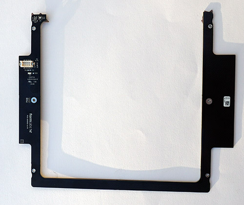
Bottom view of the mechanical platform showing the protective shrouds hiding the optics.

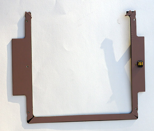
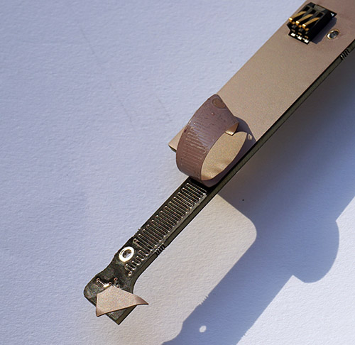
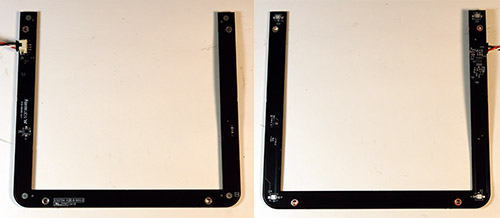
Immediately underneath the protective glass sheet is a U-shaped PCB which I can only assume is used for some kind of calibration. The PCB features five phtoodetectors; one mounted in “plain sight” of the laser, and four mounted in the far corners on the reverse side of the PCB, with the detectors facing into the PCB, such that the PCB is obscuring the photodetectors. A single, small pinhole located in the center of each detector allows light to fall onto the obscured photodetectors. However, the size of the pinhole and the dimensional tolerance of the PCB is probably too large for this to be an absolute calibration for the printer. My guess is this is probably used as more of a coarse diagnostic to confirm laser power and range of motion of the galvanometers.

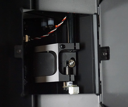
Popping off the shroud reveals the galvanometer and laser assembly. The galvanometers sport a prominent Formlabs logo. They are a Formlabs original design, and not simply a relabeling of an off the shelf solution. This is a really smart move, especially in the face of increasing pressure from copycats. Focusing resources into building a proprietary galvo is a trifecta for Formlabs: they get distinguished print quality, reduced cost, and a barrier to competition all in one package. Contrast this to Formlabs’ decision to use a SOM for the CPU; if Formlabs can build their own galvo & driver board, they certainly had the technical capability to integrate a CPU into the mainboard. But in terms of priorities, improving the galvo is a much better payout.
Readers unfamiliar with galvanometers may want to review a Name that Ware I did of a typical galvanometer a while back. In a nutshell, a typical galvanometer consists of a pair of voice coils rotating a permanent magnet affixed to a shaft. The shaft’s angle is measured by an optical feedback system, where a single light source shines onto a paddle affixed to the galvo’s shaft. The paddle alternately occludes light hitting a pair of photodetectors positioned behind the paddle relative to the light source.
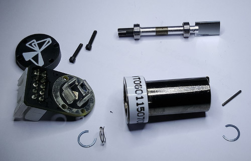
Now, here’s the entire Form 2 galvo assembly laid out in pieces.


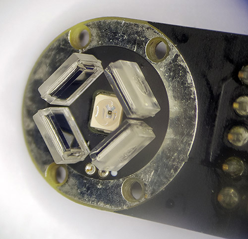
Close-up view of the photoemitter and detector arrangement.
Significantly, the Form 2 galvo has not two, but four photodetectors, surrounding a single central light source. Instead of a paddle, a notch is cut into the shaft; the notch modulates the light intensity reaching the photodiodes surrounding the central light source according to the angle of the shaft.

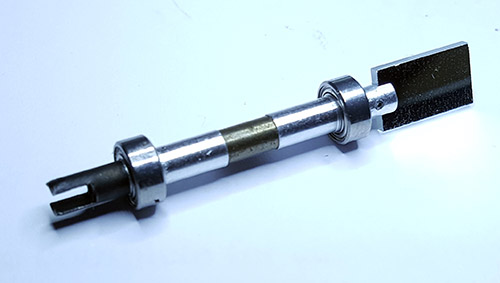
The notched shaft above sits directly above the photoemitter when the PCB is mated to the galvo body.
This is quite different from the simple galvanometer I had taken apart previously. I don’t know enough about galvos to recognize if this is a novel technique, or what exactly is the improvement they hoped to get by using four photodiodes instead of two. With two photodiodes, you get to subtract out the common mode of the emitter and you’re left with the error signal representing the angle of the shaft: two variables solving for two unknowns. With four photodiodes, they can solve for a couple more unknowns – but what are they? Maybe they are looking to correct for alignment errors of the light source & photodetectors relative to the shaft, wobble due to imperfections in the bearings, or perhaps they’re trying to avoid a dead-spot in the response of the photodiodes as the shaft approaches the extremes of rotation. Or perhaps the explanation is as simple as removing the light-occluding paddle reduces the mass of the shaft assembly, allowing it to rotate faster, and four photodetectors was required to produce an accurate reading out of a notch instead of the paddle. When I reached out to Formlabs to ask about this, someone in the know responded that the new design is an improvement on three issues: more signal leading to an improved SNR, reduced impact of off-axis shaft motion, and reduced thermal drift due to better symmetry.

This is the shaft plus bearings once it’s pulled out of the body of the galvo. The gray region in the middle is the permanent magnet, and it’s very strong.

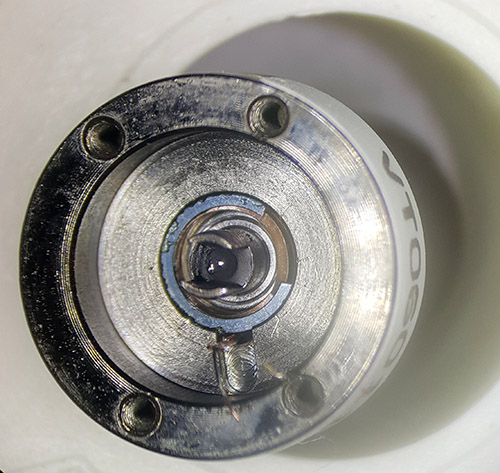
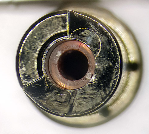
And this is staring back into the galvo with the shaft removed. You can see the edges of the voice coils. I couldn’t remove them from the housing, as they seem to be fixed in place with some kind of epoxy.
Epilogue
And there you have it – the Form 2, from taking off its outer metal case down to the guts of its galvanometers. It was a lot of fun tearing down the Form2, and I learned a lot while doing it. I hope you also enjoyed reading this post, and perhaps gleaned a couple useful bits of knowledge along the way.
If you think Formlabs is doing cool stuff and solving interesting problems, good news: they’re hiring! They have new positions for a Software Lead and an Electrical Systems Lead. Follow the links for a detailed description and application form.
