The ware for January is shown below.
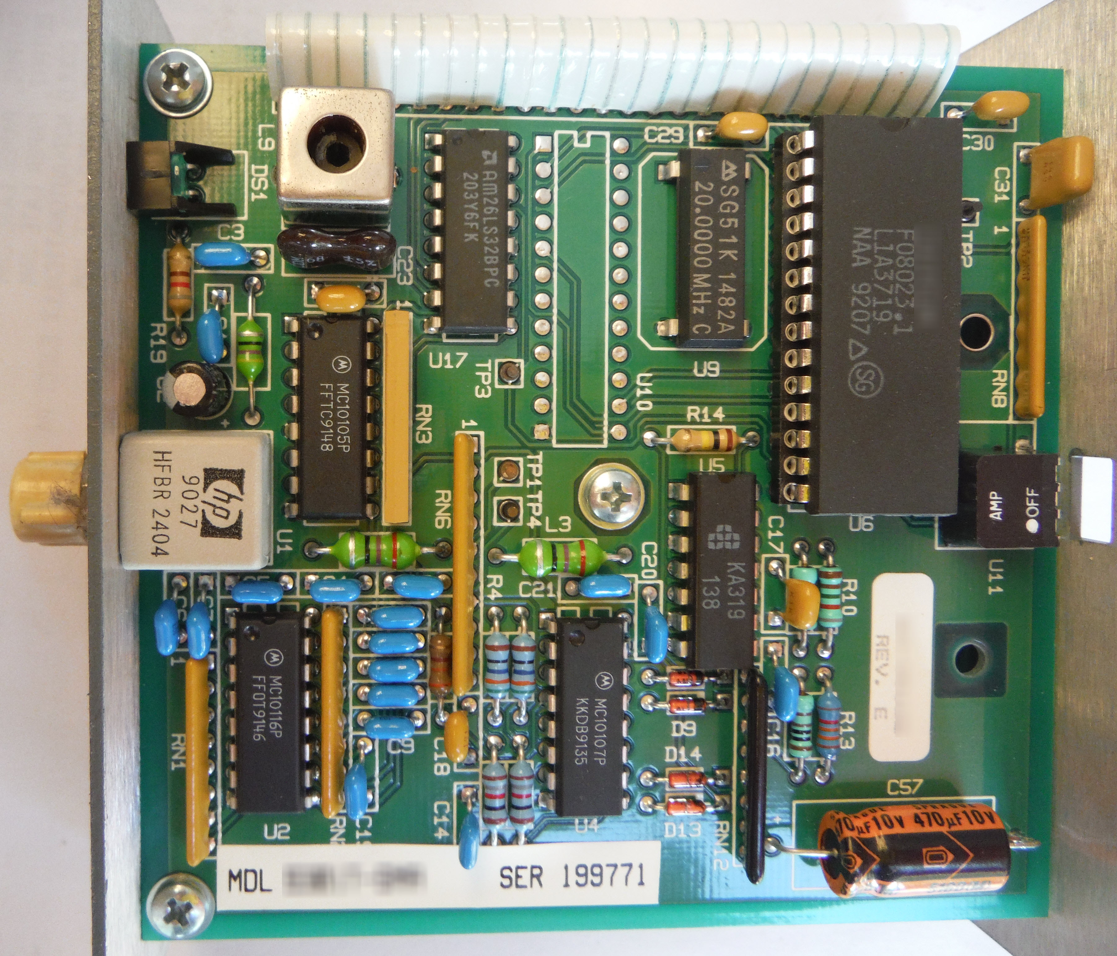
Thanks to my buddy Mike Fitzmorris for contributing yet another wonderful ware to this competition.
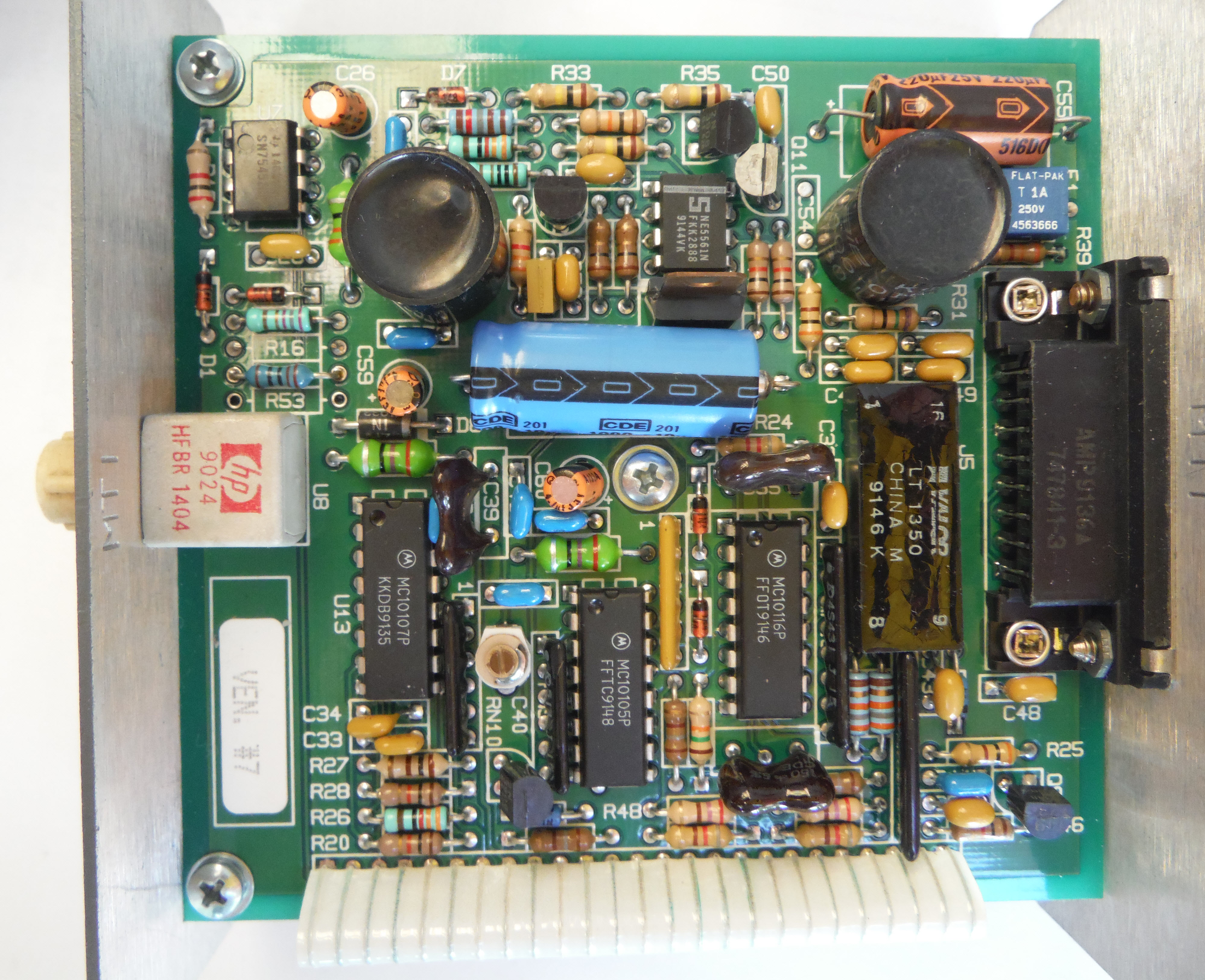
The ware for January is shown below.
Thanks to my buddy Mike Fitzmorris for contributing yet another wonderful ware to this competition.
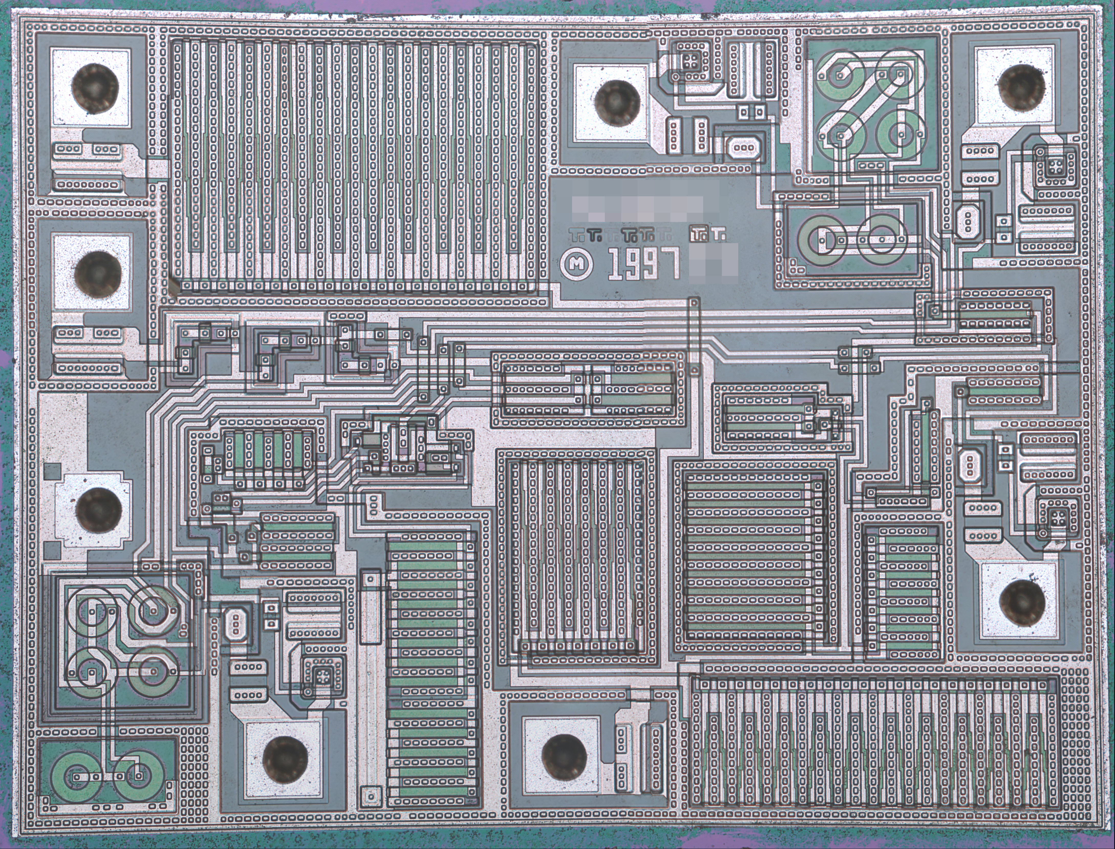
The Ware for last December 2013 is the beloved 555 timer, specifically the TLC555 by TI, fabricated in their “LinCMOS” process. I was very excited when T. Holman allowed me to post this as a ware, partially because I love die shots, and partially because the 555 is such a noteworthy chip and up until now I had never seen the inside of one.
The huge transistor on the top left is the discharge N-FET, and the distinctive, round FETs are I believe what makes LinCMOS special. These are tailor-designed transistors for good matching across process conditions, and they form the front ends of the two differential comparators that are the backbone of the threshold/trigger circuit inside the 555.
Picking a winner this time was tough — many close guesses. I’m going to name “eric” the winner, as he not only properly identified the chip, but also gave extensive analysis in his answer as well. DavidG had a correct guess very early on, but no explanation. Jonathan had the right answer, but the divider underneath the big transistor wasn’t done with resistors, it’s done with FETs, and steveM2 also was very, very close but called it a TLC551Y. So congrats to eric, email me to claim your prize.
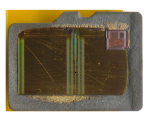
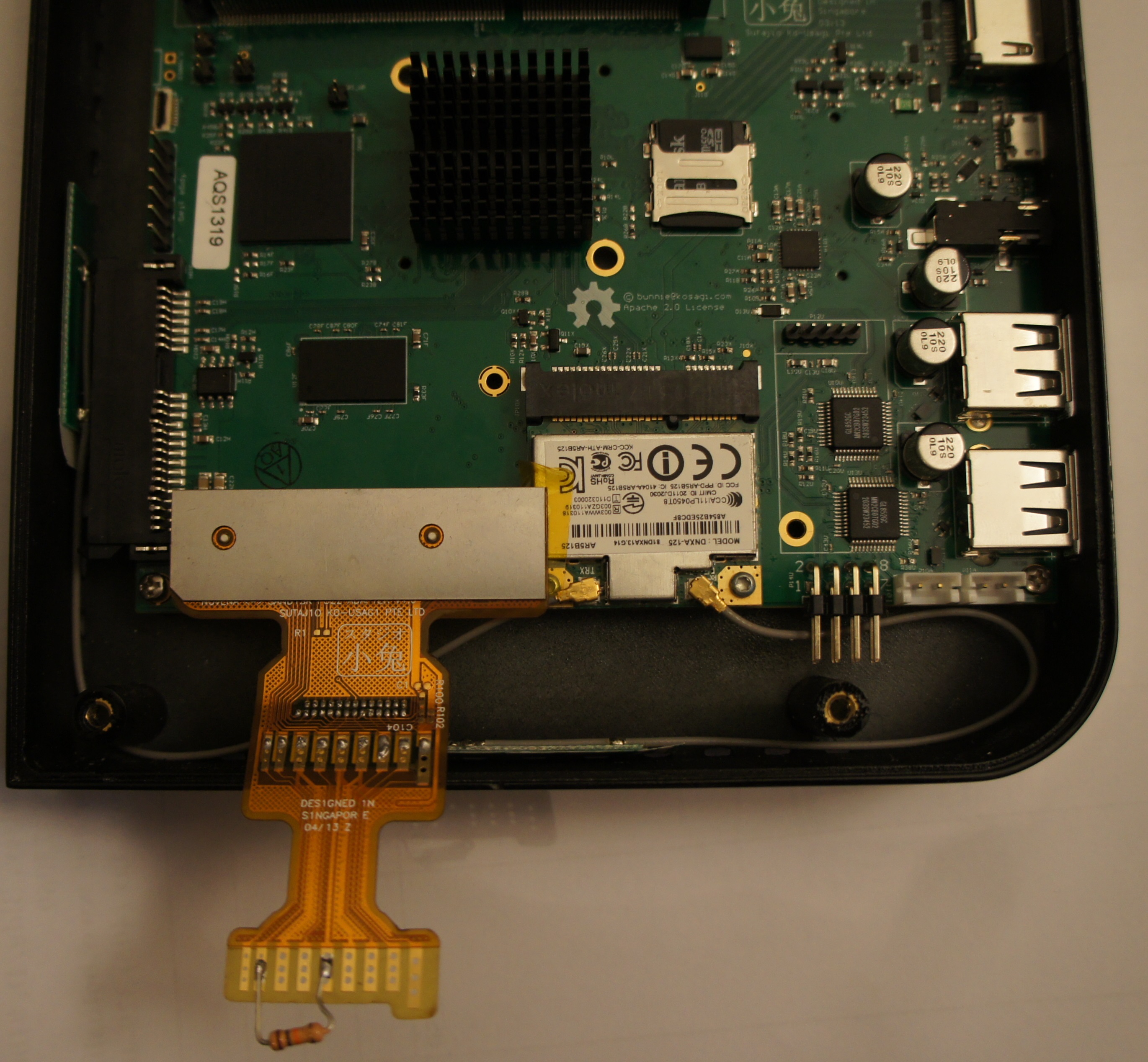
Today at the Chaos Computer Congress (30C3), xobs and I disclosed a finding that some SD cards contain vulnerabilities that allow arbitrary code execution — on the memory card itself. On the dark side, code execution on the memory card enables a class of MITM (man-in-the-middle) attacks, where the card seems to be behaving one way, but in fact it does something else. On the light side, it also enables the possibility for hardware enthusiasts to gain access to a very cheap and ubiquitous source of microcontrollers.
In order to explain the hack, it’s necessary to understand the structure of an SD card. The information here applies to the whole family of “managed flash” devices, including microSD, SD, MMC as well as the eMMC and iNAND devices typically soldered onto the mainboards of smartphones and used to store the OS and other private user data. We also note that similar classes of vulnerabilities exist in related devices, such as USB flash drives and SSDs.
Flash memory is really cheap. So cheap, in fact, that it’s too good to be true. In reality, all flash memory is riddled with defects — without exception. The illusion of a contiguous, reliable storage media is crafted through sophisticated error correction and bad block management functions. This is the result of a constant arms race between the engineers and mother nature; with every fabrication process shrink, memory becomes cheaper but more unreliable. Likewise, with every generation, the engineers come up with more sophisticated and complicated algorithms to compensate for mother nature’s propensity for entropy and randomness at the atomic scale.
These algorithms are too complicated and too device-specific to be run at the application or OS level, and so it turns out that every flash memory disk ships with a reasonably powerful microcontroller to run a custom set of disk abstraction algorithms. Even the diminutive microSD card contains not one, but at least two chips — a controller, and at least one flash chip (high density cards will stack multiple flash die). You can see some die shots of the inside of microSD cards at a microSD teardown I did a couple years ago.
In our experience, the quality of the flash chip(s) integrated into memory cards varies widely. It can be anything from high-grade factory-new silicon to material with over 80% bad sectors. Those concerned about e-waste may (or may not) be pleased to know that it’s also common for vendors to use recycled flash chips salvaged from discarded parts. Larger vendors will tend to offer more consistent quality, but even the largest players staunchly reserve the right to mix and match flash chips with different controllers, yet sell the assembly as the same part number — a nightmare if you’re dealing with implementation-specific bugs.
The embedded microcontroller is typically a heavily modified 8051 or ARM CPU. In modern implementations, the microcontroller will approach 100 MHz performance levels, and also have several hardware accelerators on-die. Amazingly, the cost of adding these controllers to the device is probably on the order of $0.15-$0.30, particularly for companies that can fab both the flash memory and the controllers within the same business unit. It’s probably cheaper to add these microcontrollers than to thoroughly test and characterize each flash memory chip, which explains why managed flash devices can be cheaper per bit than raw flash chips, despite the inclusion of a microcontroller.
The downside of all this complexity is that there can be bugs in the hardware abstraction layer, especially since every flash implementation has unique algorithmic requirements, leading to an explosion in the number of hardware abstraction layers that a microcontroller has to potentially handle. The inevitable firmware bugs are now a reality of the flash memory business, and as a result it’s not feasible, particularly for third party controllers, to indelibly burn a static body of code into on-chip ROM.
The crux is that a firmware loading and update mechanism is virtually mandatory, especially for third-party controllers. End users are rarely exposed to this process, since it all happens in the factory, but this doesn’t make the mechanism any less real. In my explorations of the electronics markets in China, I’ve seen shop keepers burning firmware on cards that “expand” the capacity of the card — in other words, they load a firmware that reports the capacity of a card is much larger than the actual available storage. The fact that this is possible at the point of sale means that most likely, the update mechanism is not secured.
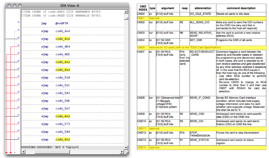
In our talk at 30C3, we report our findings exploring a particular microcontroller brand, namely, Appotech and its AX211 and AX215 offerings. We discover a simple “knock” sequence transmitted over manufacturer-reserved commands (namely, CMD63 followed by ‘A’,’P’,’P’,’O’) that drop the controller into a firmware loading mode. At this point, the card will accept the next 512 bytes and run it as code.
From this beachhead, we were able to reverse engineer (via a combination of code analysis and fuzzing) most of the 8051’s function specific registers, enabling us to develop novel applications for the controller, without any access to the manufacturer’s proprietary documentation. Most of this work was done using our open source hardware platform, Novena, and a set of custom flex circuit adapter cards (which, tangentially, lead toward the development of flexible circuit stickers aka chibitronics).
Significantly, the SD command processing is done via a set of interrupt-driven call backs processed by the microcontroller. These callbacks are an ideal location to implement an MITM attack.
It’s as of yet unclear how many other manufacturers leave their firmware updating sequences unsecured. Appotech is a relatively minor player in the SD controller world; there’s a handful of companies that you’ve probably never heard of that produce SD controllers, including Alcor Micro, Skymedi, Phison, SMI, and of course Sandisk and Samsung. Each of them would have different mechanisms and methods for loading and updating their firmwares. However, it’s been previously noted that at least one Samsung eMMC implementation using an ARM instruction set had a bug which required a firmware updater to be pushed to Android devices, indicating yet another potentially promising venue for further discovery.
From the security perspective, our findings indicate that even though memory cards look inert, they run a body of code that can be modified to perform a class of MITM attacks that could be difficult to detect; there is no standard protocol or method to inspect and attest to the contents of the code running on the memory card’s microcontroller. Those in high-risk, high-sensitivity situations should assume that a “secure-erase” of a card is insufficient to guarantee the complete erasure of sensitive data. Therefore, it’s recommended to dispose of memory cards through total physical destruction (e.g., grind it up with a mortar and pestle).
From the DIY and hacker perspective, our findings indicate a potentially interesting source of cheap and powerful microcontrollers for use in simple projects. An Arduino, with its 8-bit 16 MHz microcontroller, will set you back around $20. A microSD card with several gigabytes of memory and a microcontroller with several times the performance could be purchased for a fraction of the price. While SD cards are admittedly I/O-limited, some clever hacking of the microcontroller in an SD card could make for a very economical and compact data logging solution for I2C or SPI-based sensors.
Slides from our talk at 30C3 can be downloaded here, or you can watch the talk on Youtube below.
Team Kosagi would like to extend a special thanks to .mudge for enabling this research through the Cyber Fast Track program.
The Ware for December 2013 is shown below.
It’s been a while since I’ve had a proper die shot for a name that ware. Thanks to T. Holman for sharing this ware with us!
[Edit: You can download a copy of the original, unobfuscated image here (warning: 23MB).]
The Ware for November 2013 is anisotropic conductive tape, aka “Z-tape”. When I first heard about Z-tape, I scratched my head and wondered how that could work; but after lighting it up under a microscope, I instantly had a clear intuition for how it works, and its limitations.
The winner for last month’s competition is Scott Roberts, who for the record entered the correct guess prior to the answer being posted a couple days later in a follow-up post about circuit stickers. Congrats, email me for your prize!