I got a Form 1 3D printer!
It’s the first 3D printer I’ve purchased (technically, I “backed” it). I managed to acquire a pre-release beta unit, as I’m affiliated with Neoteny Labs, one of Formlabs’ investors.
What’s the first thing I do with any shiny new gadget? That’s right, I take it apart!
Unboxing
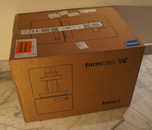
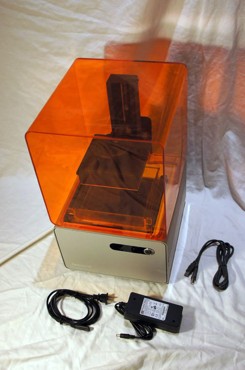
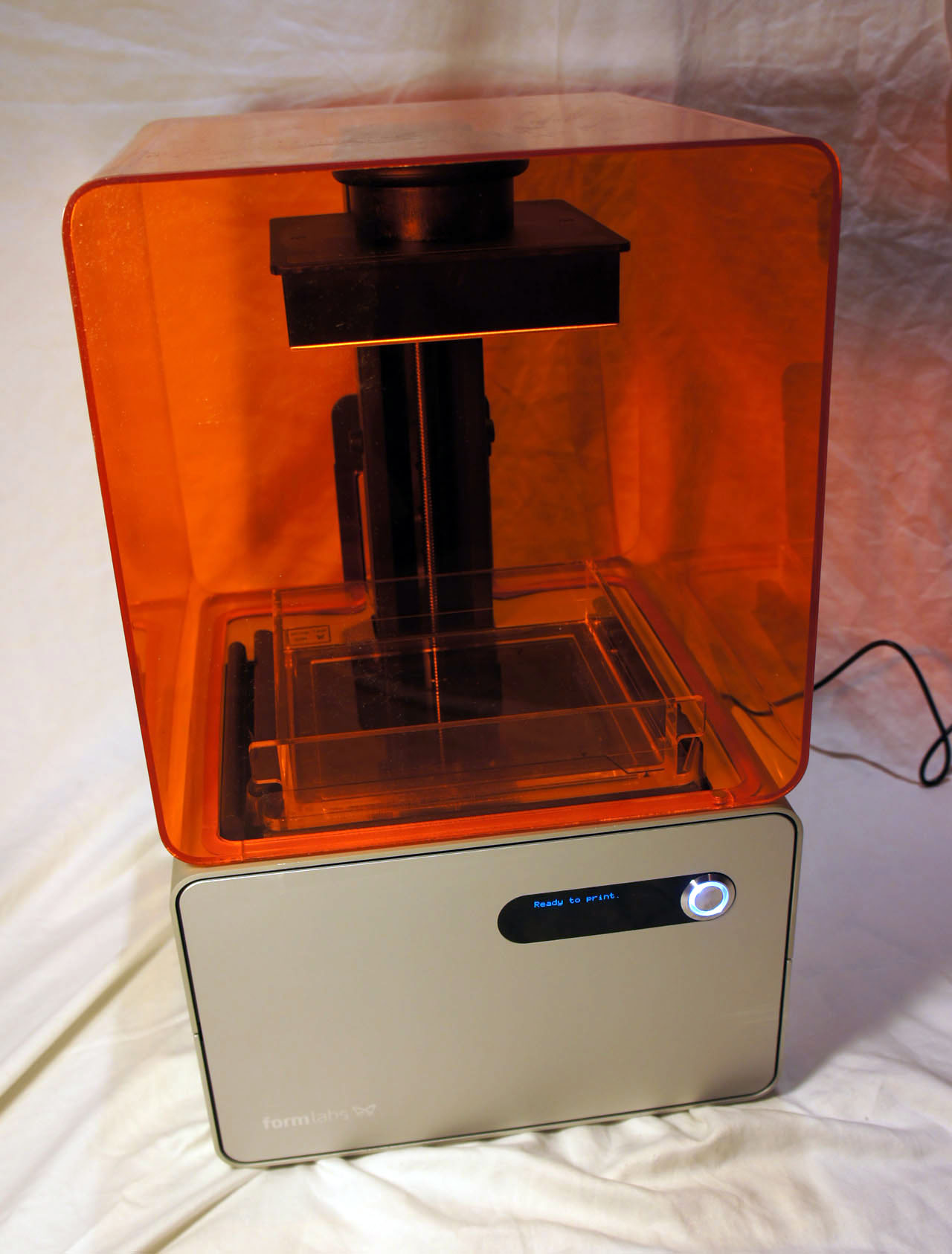
The complete Form 1 kit consists of three boxes: the printer (shown above), bottles of liquid photocurable resin, and a cleaning station. Many optical stereolithography printers require a cleaning step to wash off the uncured resin; for the Form 1 this means rinsing the part in isopropyl alcohol (the same stuff you use to disinfect cuts, but more concentrated) for a few minutes.
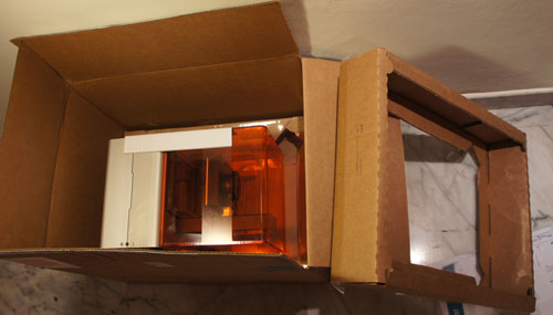
The packing method, at least for the beta, is styrofoam-free. It uses a pair of thin plastic sheets suspended on cardboard frames to hold the printer in a cradle. For a box that went as checked luggage from Boston to Singapore through three flights, it held up remarkably well.

The printer box also contains the power supply, cables, and the requisite quickstart guides.

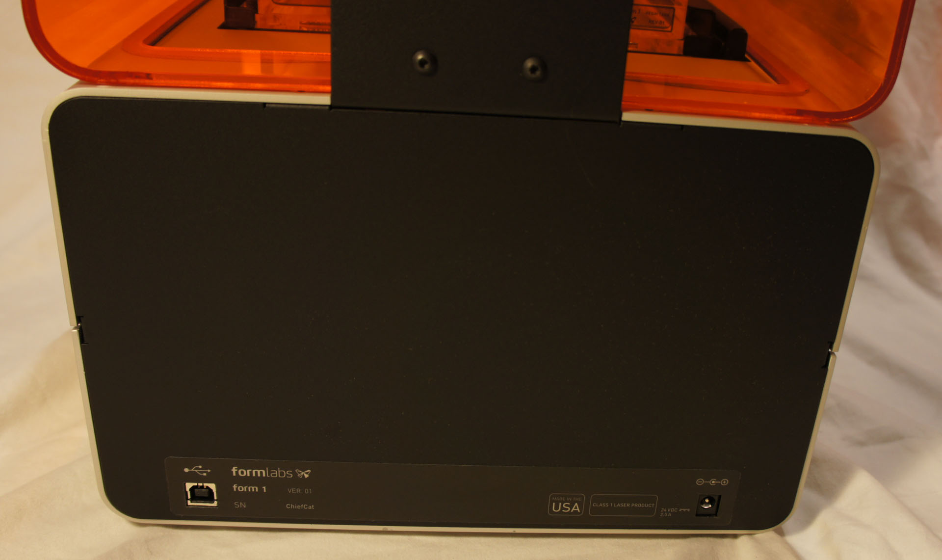
The serial number scheme, at least for the beta units, is “AdjectiveAnimalname”, so mine is simply “ChiefCat” — hurray for easy-to-read serial numbers!
Undressing
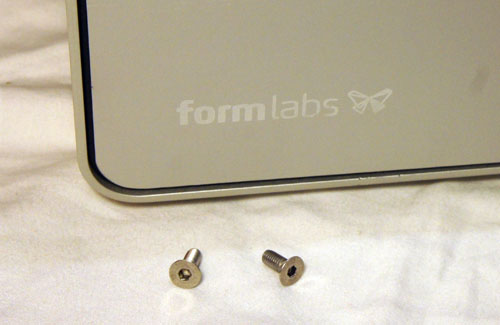
You need exactly one tool to disassemble the printer: a 2.5mm hex key (or, if you’re a fan of Torx, a T-10 bit). I really appreciate the balance of good design with practicality: it looks good, and you don’t need whacky pentalobe screwdrivers to service it. It does take a bit of elbow grease to undo the screws; but a grippy Torx driver makes short work of the problem without a single stripped screw.

Two screws release the orange-colored light shield from its hinge, and four screws release the top of the base unit from the frame. The orange-colored shield protects your eyes from stray blue laser light, while also protecting the photosensitive resin bath on the inside from stray ambient light.

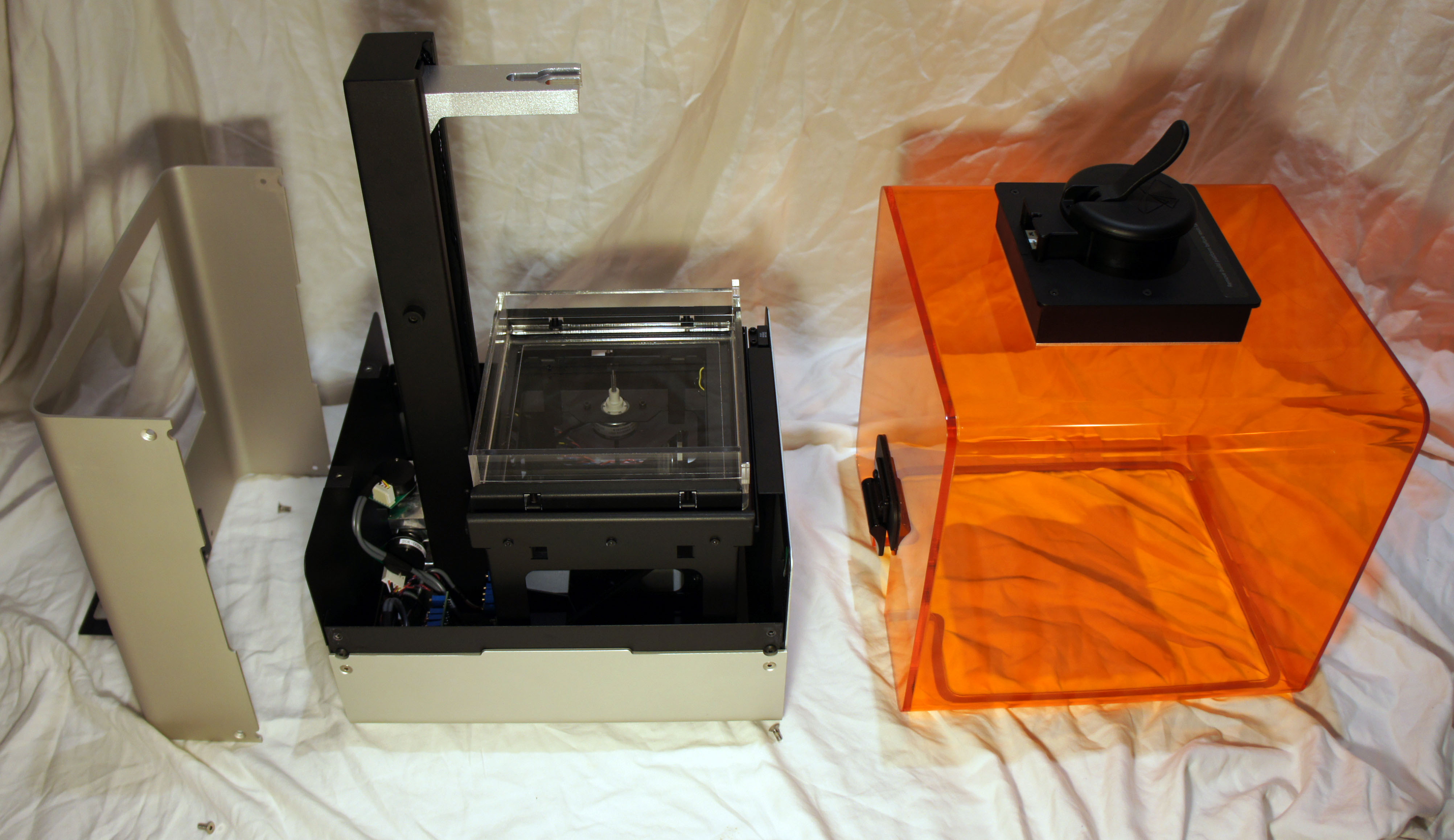
Six more screws (two of which are on the bottom) release the mid-frame from the base. The mid-frame is screwed to the front and back panels, but I didn’t need to remove the panels, as there is enough flexability in the sheet aluminum to slide the mid-frame off. The wiring to the front panel is tidily secured and is exactly the right length to allow the frame to sit next to the base without having to undo any cables — super-convenient for service and debug.

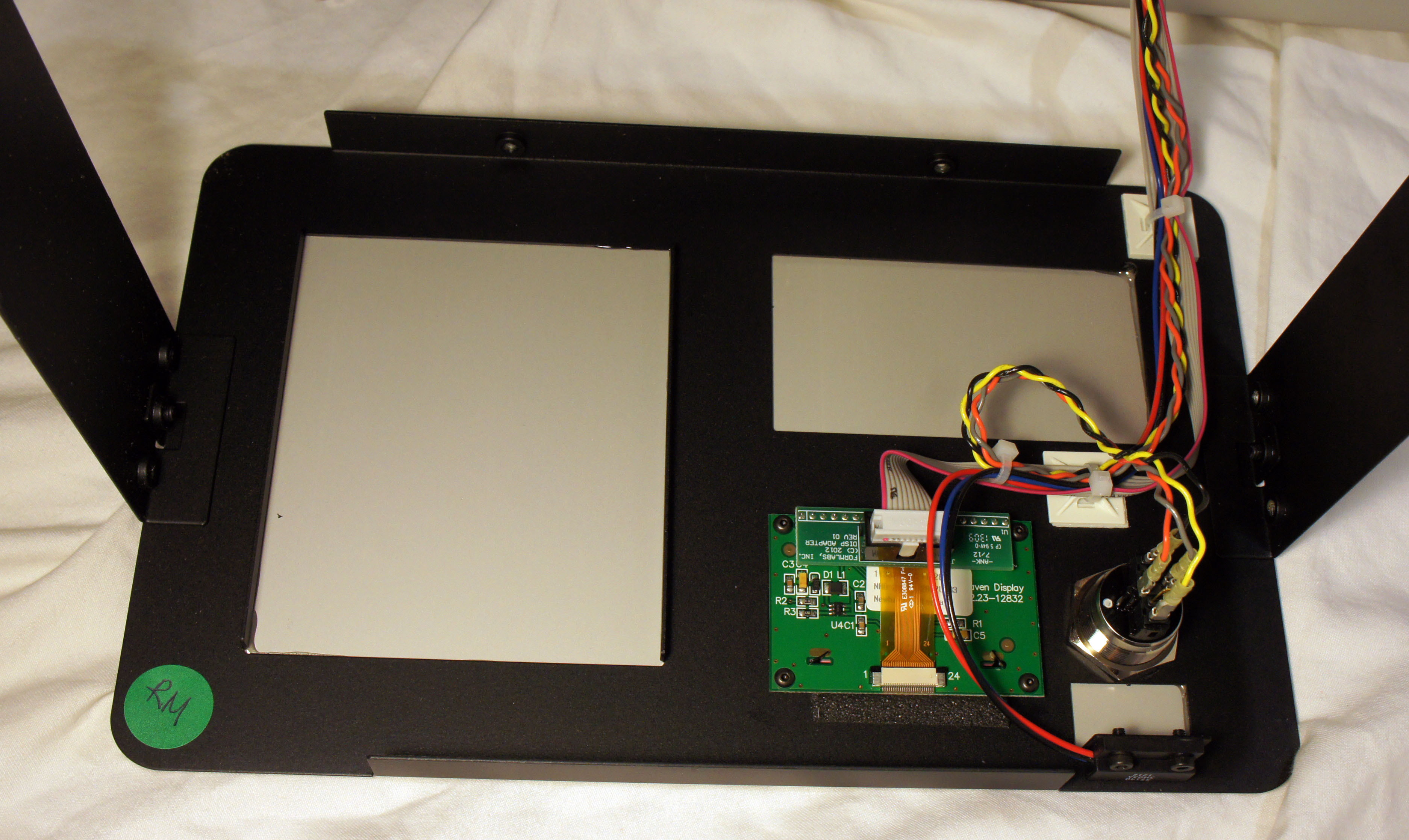
The inside of the front panel reveals the adapter for the OLED display, as well as the very handsome back-lit power button.
The Mechanism
One of the great things about a stereolithography 3D printer is that it uses a laser to cure a resin, instead of melting and extruding a plastic. As a result, the operation is whisper-quiet, and there is no odor during operation — you can put the printer in a bedroom and still sleep at night. To borrow the words of Obi-Wan Kenobi: “This is the 3D printer of a Jedi Knight. Not as clumsy or as random as an FDM, but an elegant tool for a more civilized age.”
I count four motors in the Form 1: two stepper motors with lead screws, and two galvonometers (which I refer to as simply “galvos”). Let’s tour the printer’s mechanisms, motor by motor.
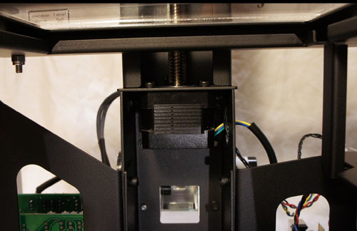
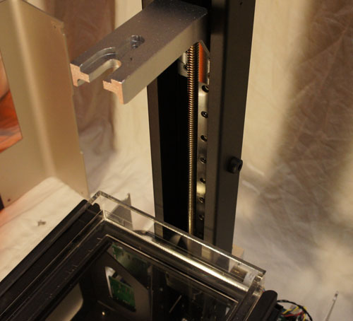
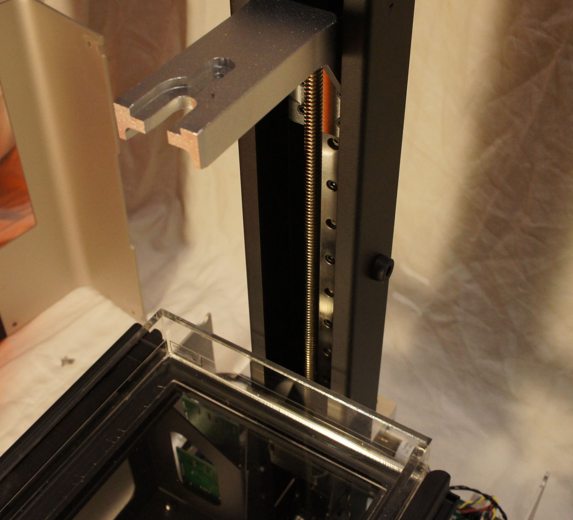
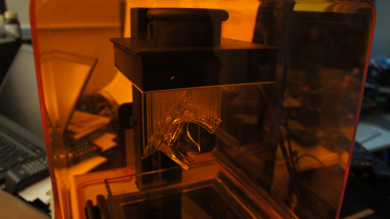
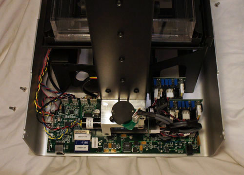
A large stepper motor with a lead screw running up the spine of the device pulls the build platform upwards. This causes the printed object to appear to “grow” out of the resin bath.
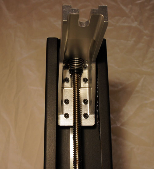
The build platform is attached to the leadscrew with an anti-backlash nut. The spring in the picture above applies a static force to the leadscrew-nut interface, reducing the play between the two and improving accuracy.

Every time a thin layer of resin is cured, a second motor performs a “peel” operation by tilting one edge of the resin tank downwards. The peel operation separates the newly formed layer from the bottom of the resin tank, allowing the build platform to move up freely. The leadscrew pictured above is responsible for this action, and it is driven by the smaller of two motors inside the Form 1. The white bearing is fixed to the frame, and the pin connecting the leadscrew to the tiltable resin tank is visible at the top.

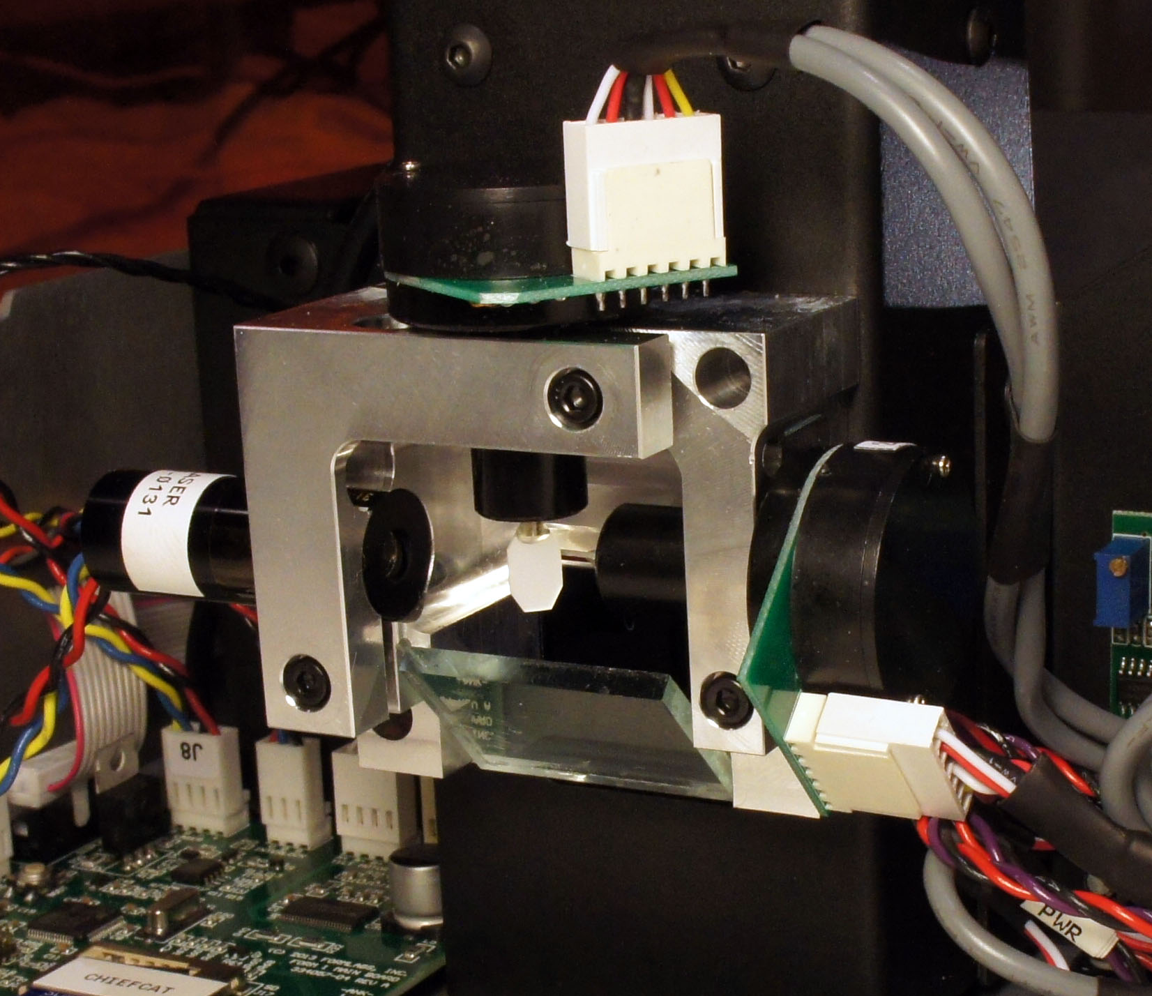
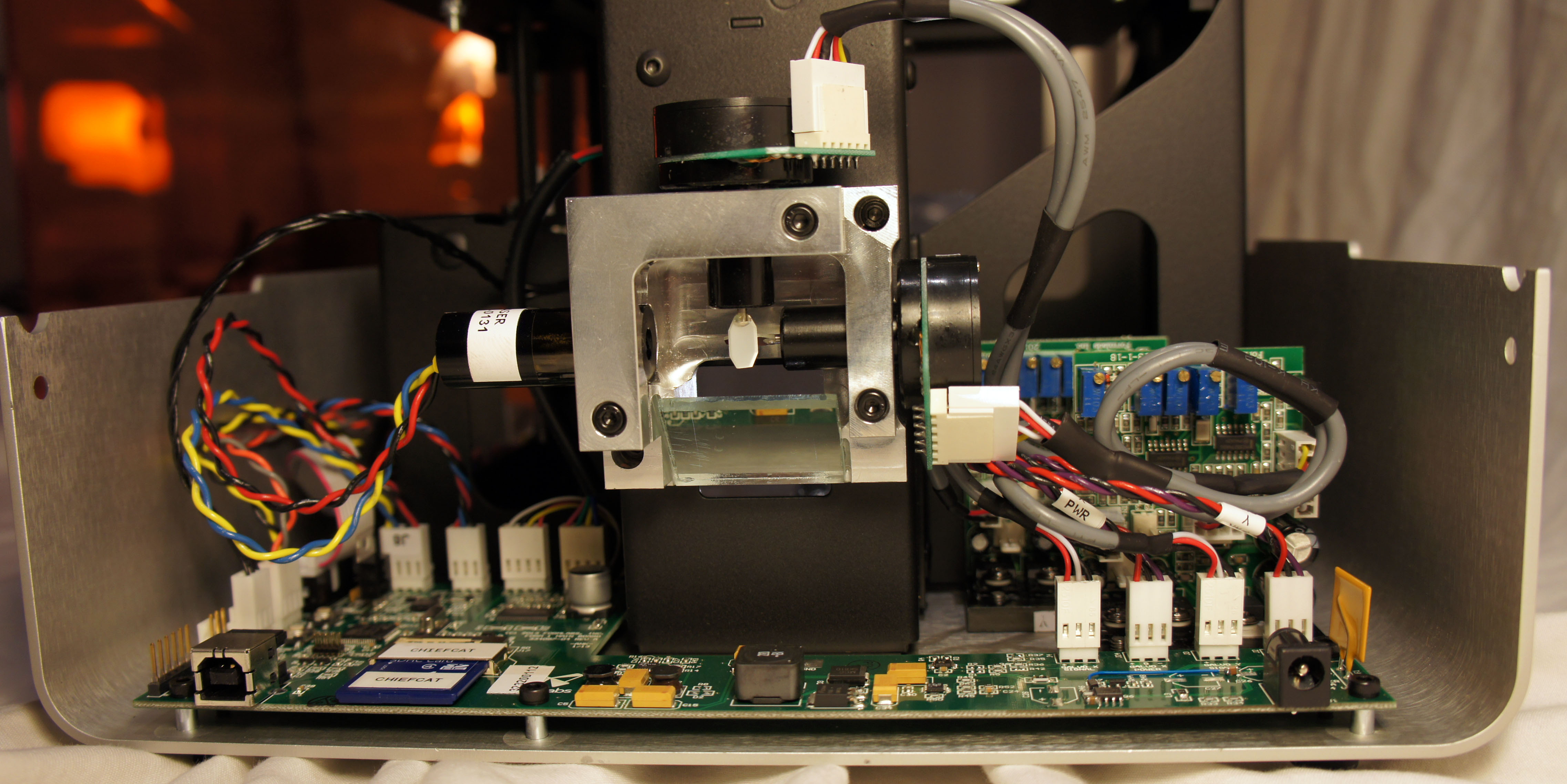
Ah…and now we peer into the heart of the Form 1! Here are the two remaining motors of the Form 1, the galvos. Galvos are very precise rotational actuators, with a built-in optical feedback loop (take a look inside one). The galvos each have a tiny octagonal mirror attached to their shafts, and are mounted at right angles to each other. One galvo steers the laser beam, entering from the left, along the X axis; then the light bounces to a second galvo that steers along the Y axis. The two working together can thus trace the 2-D vector pattern used to cure a single layer of resin. Below the galvos and laser is a mirror that reflects the light to another, larger mirror that finally shines the beam upwards into the resin bath.
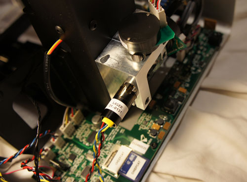
Above is another view of the laser. According to the safety warning bundled with the printer, it is a 405nm, 120mW violet laser diode (take a look inside one).
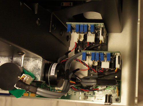
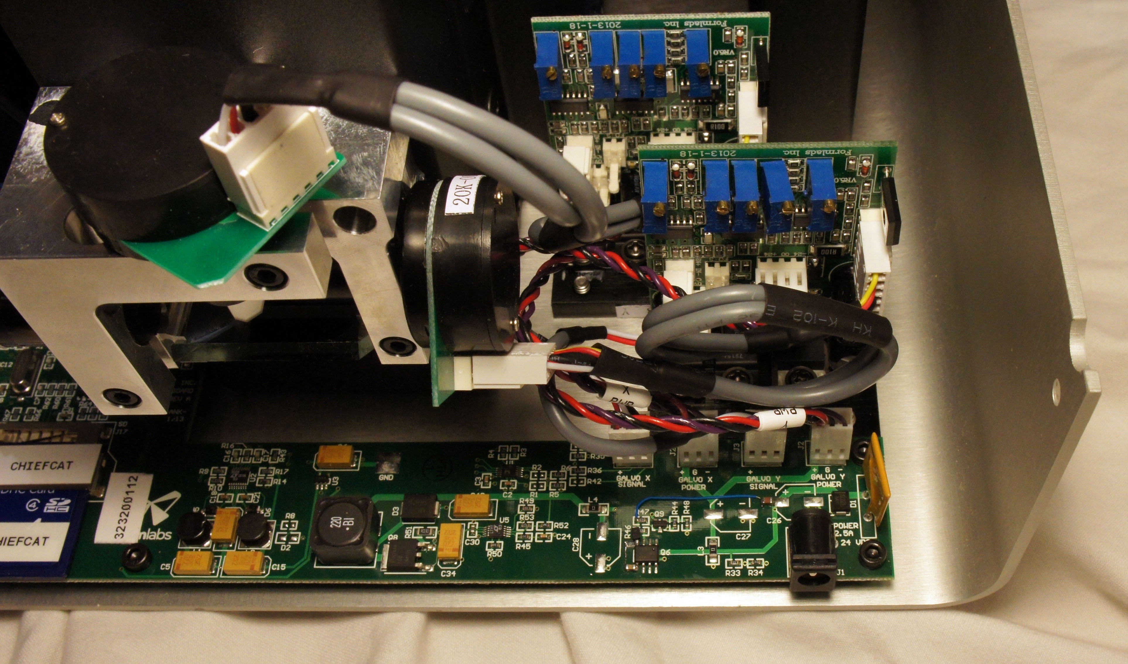
In order to achieve high performance, the galvo has a sturdy bank of drivers, mounted to the bottom aluminum surface of the case for heat sinking.
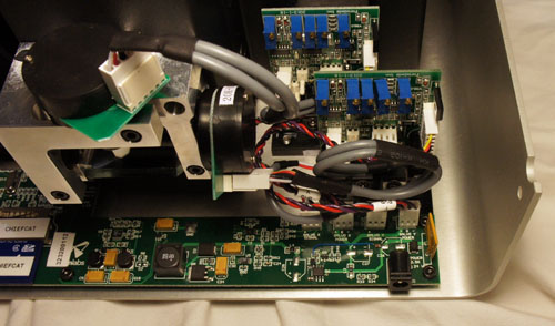
A slightly different camera angle shows the power input stage of the Form 1.
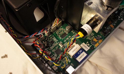
The main board wraps around the spine of the Form 1 and on the left side are the brains. An STM32 32-bit ARM Cortex-M3 microcontroller coordinates all of the activities inside the Form 1, and it appears that firmware for the device is stored on an internal, captive SD card.

Above are some photos that give the whole context of the electronics behind the Form 1.

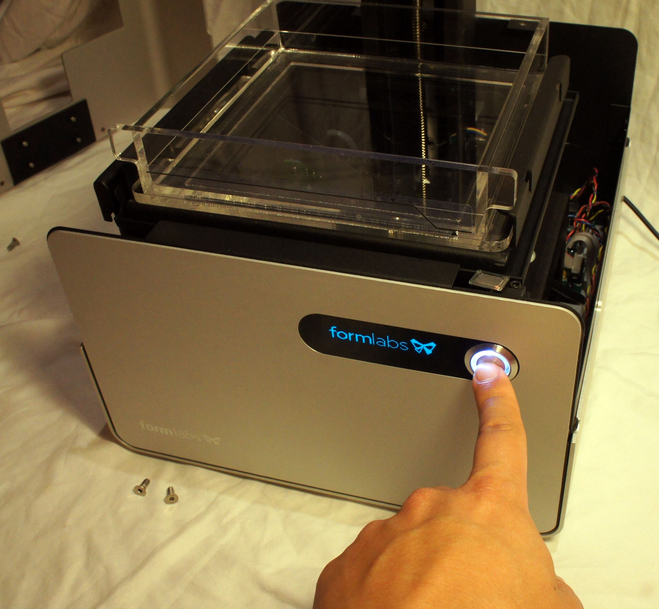
A hall effect sensor inside the base makes sure you can’t turn the device on when the protective light shield is lifted. But, you can defeat the sensor by putting a magnet on it, as I did above to check I hadn’t damaged anything before putting the whole thing back together again.

Re-assembly is a breeze — within a couple minutes I have the whole printer put back together and ready to do my first test print.
My First Print
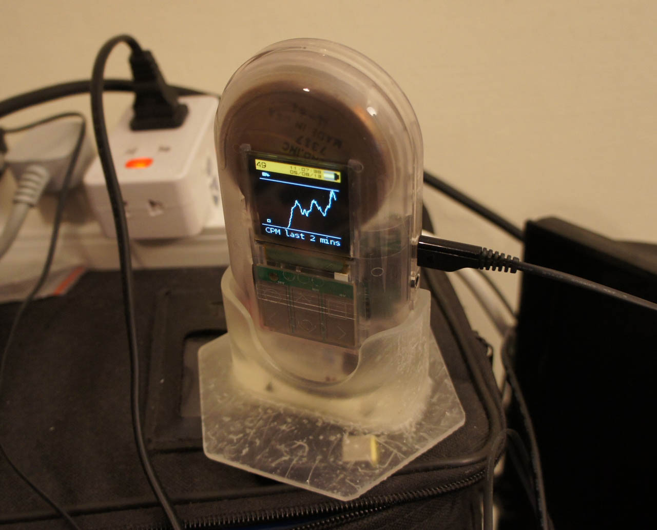
What’s the first thing I’m going to print? I’m going to download and print a stand, designed by another user (IHeartEngineering) and shared for free, for my Geiger counter!

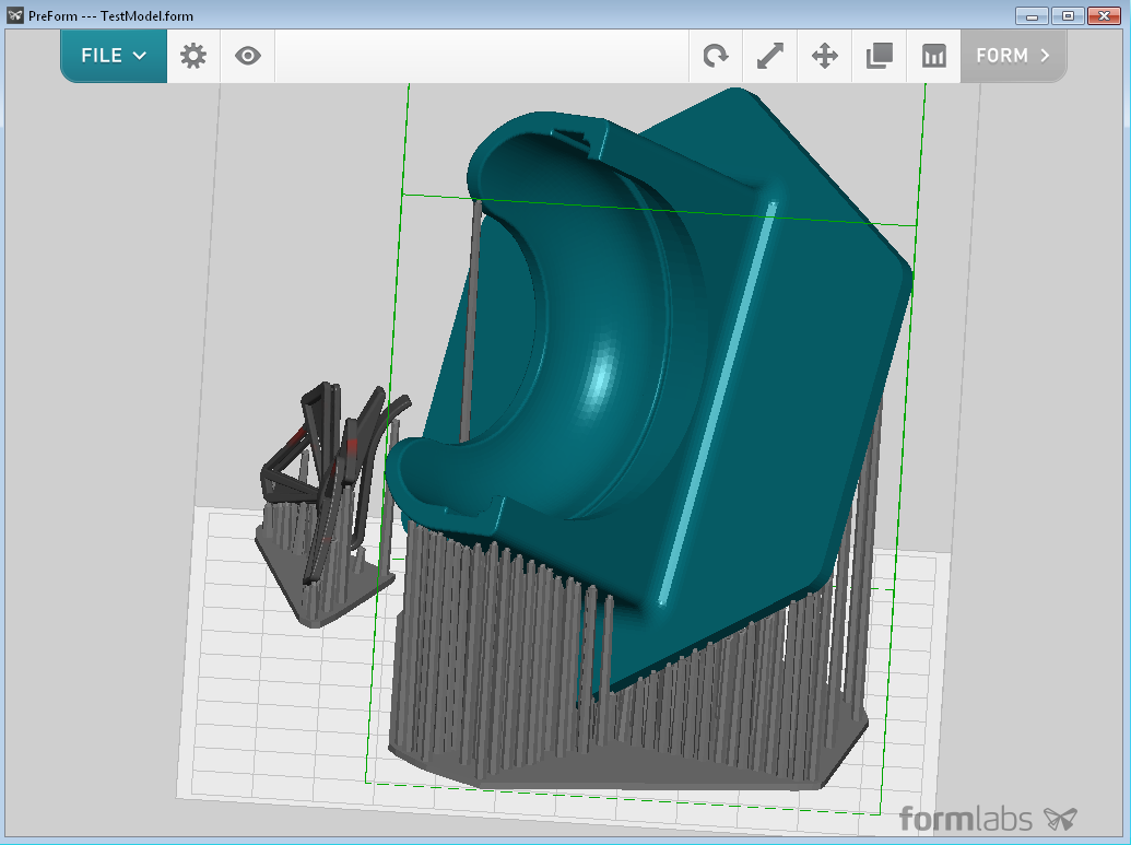
The Form 1 comes with a print management software package called “Preform”. It’s intuitive and easy to use; it allows you to place multiple objects on the build platform, duplicate, scale, and rotate. There’s an auto-orient feature that suggests an optimal orientation for supports based upon a DFM analysis. The screencap above is the result of the software picking the build orientation and populating the build supports.
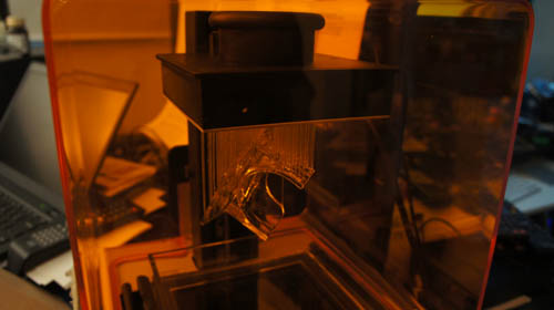
I click “Form”, and about 10 hours later the print is done.
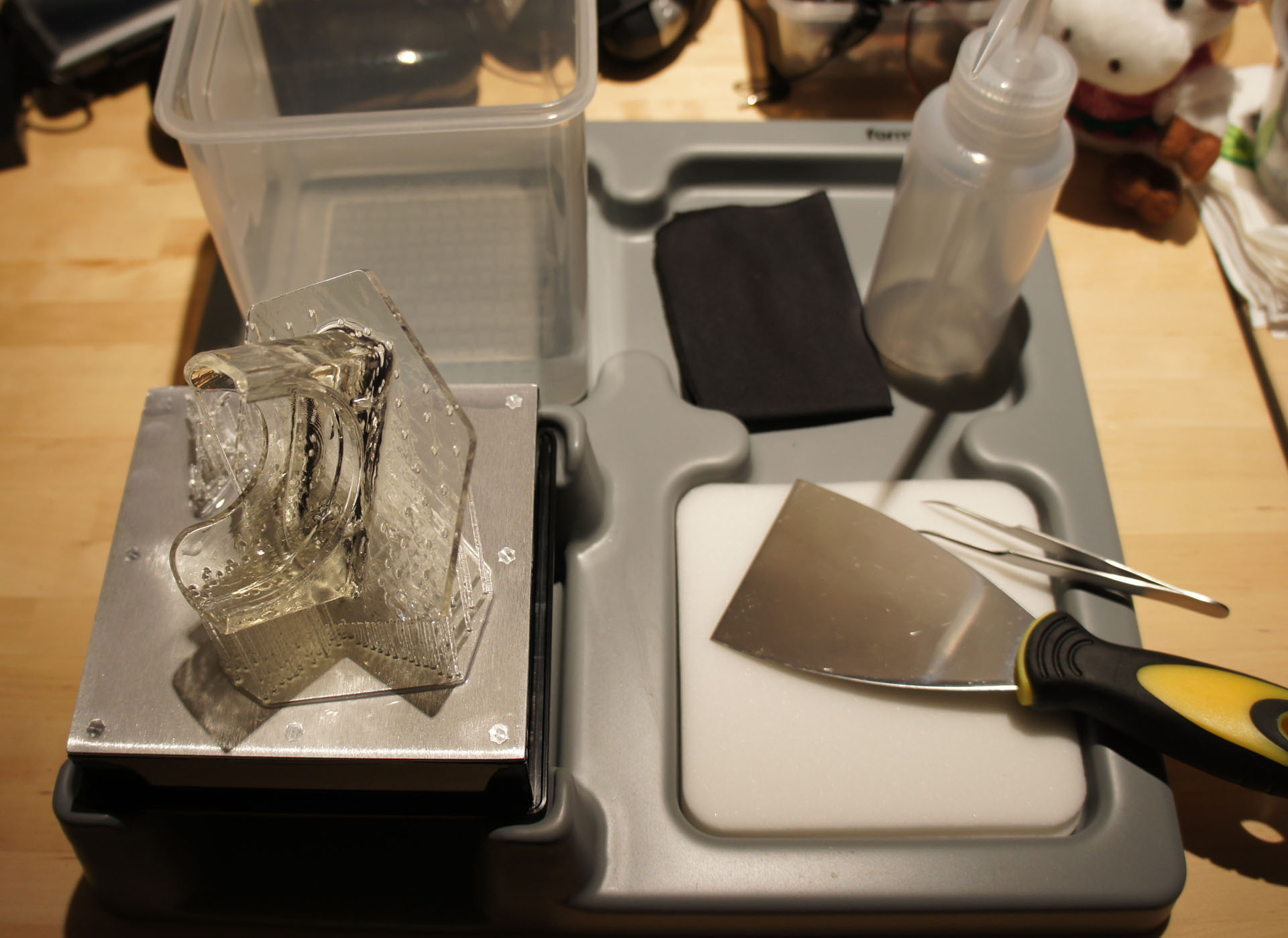
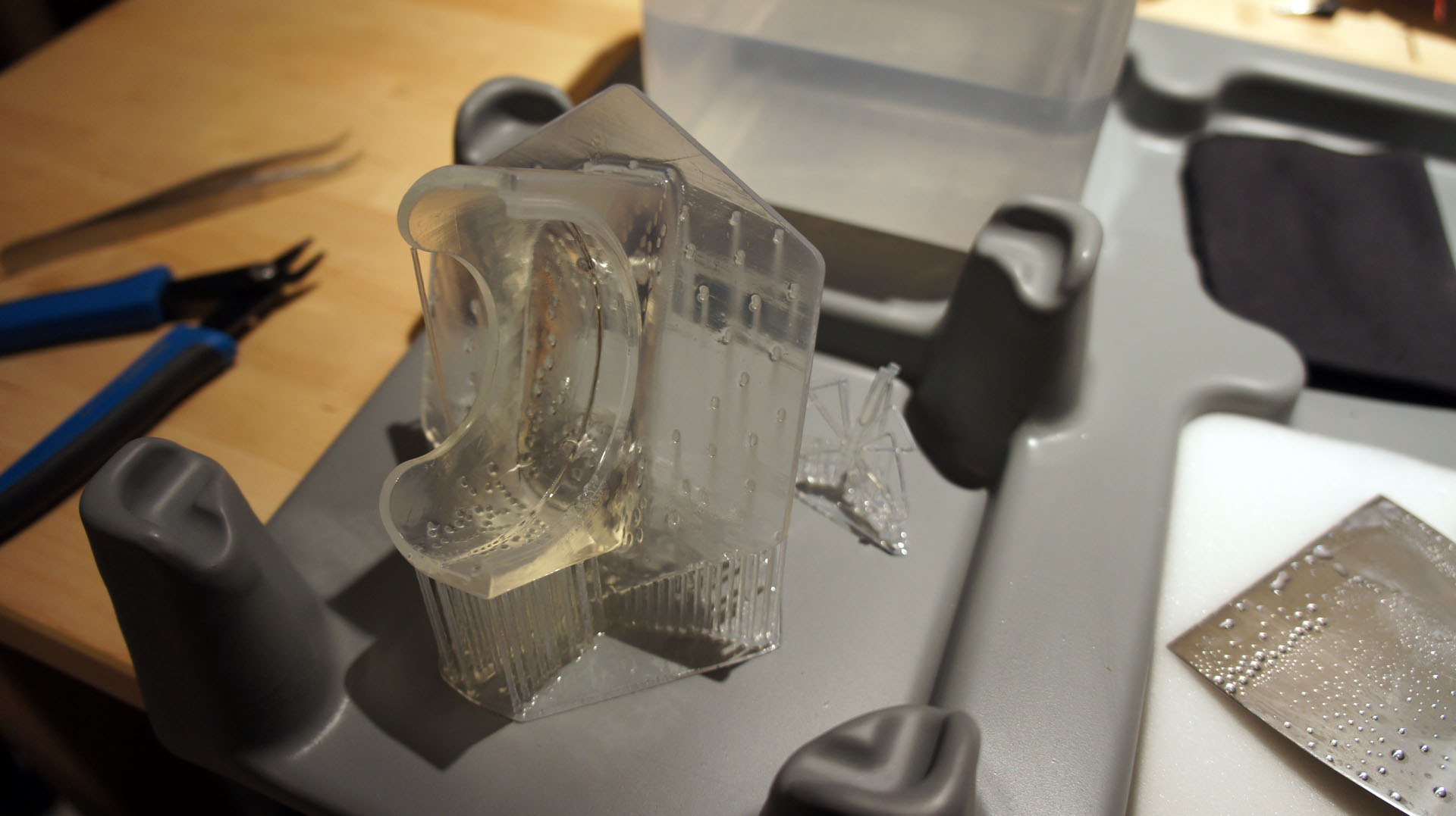
The next step is to remove the build platform from the printer and bring it to the cleaning station, one of the accessories shipped with the Form 1. Cleaning is necessary to remove uncured liquid resin residue, and it’s recommended to handle uncleaned parts using gloves to avoid getting the goopy resin on your fingers.

The cleaning station is thoughtfully laid out, with an area designed to hold the build platform. The kit includes some of the requisite tools to peel the part off of the platform, rinse it, and break off the supports. I supplement the kit with a pair of diagonal cutters for removing the supports, although you can also simply snap the supports off by pulling on them.

Two minutes of active shaking in an isopropyl bath, ten minutes of soaking, and the part is ready to be handled.

I use a pair of diagonal cutters to remove all of the supports in about five minutes.

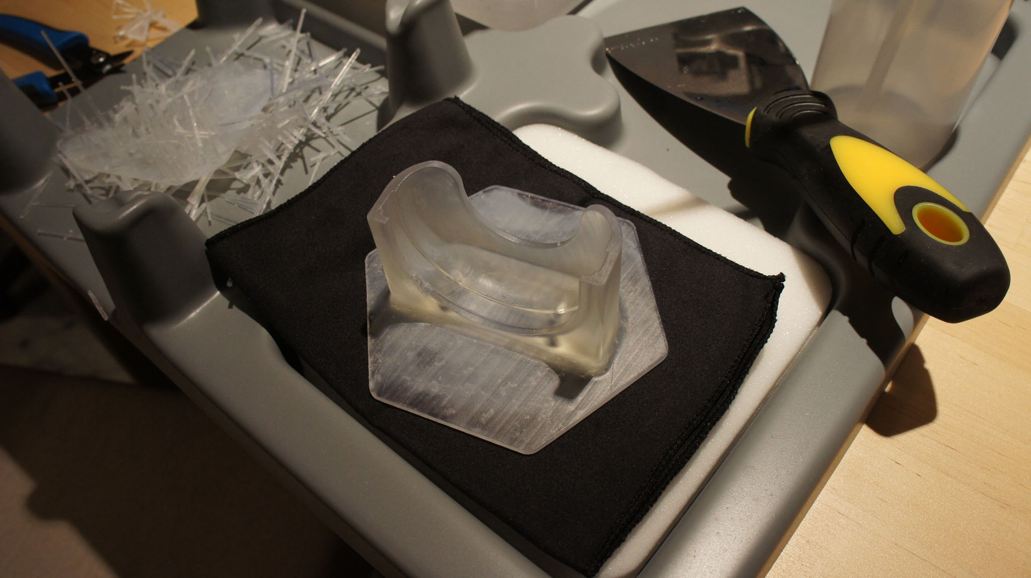
This particular part features large, robust geometries: it’s designed to be printable on an FDM, so it doesn’t show off the high-resolution capability of the Form 1.
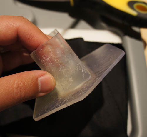
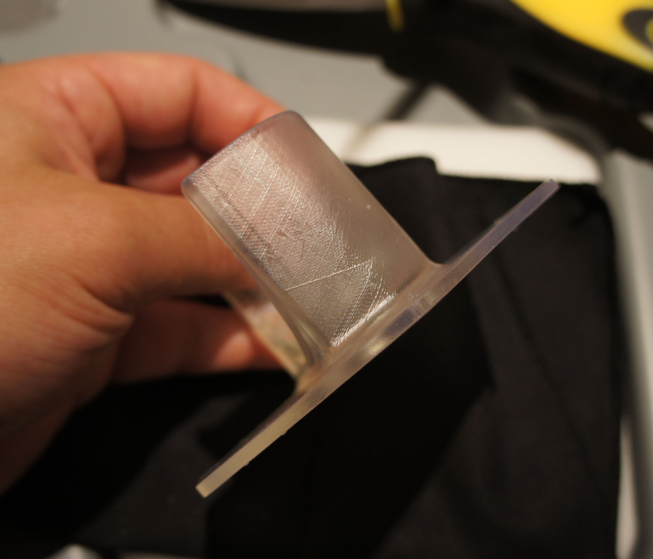
Small bumps are left on the area where the supports contact the part. These can be sanded off, if necessary.
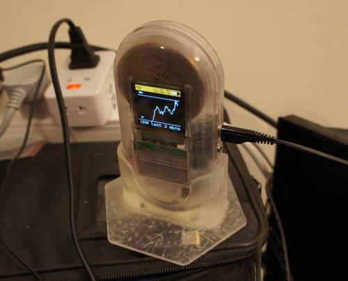
The print is a success! It fits my Geiger counter like a glove.
And now for the shameless plug: if you made it all the way through this tear-down, and you’re a top-notch EE, you might want to consider applying for Formlabs’ Electrical Engineering Lead position by dropping them an email with your resume and cover letter.