I was wandering around the Hua Qian Bei district yesterday with xobs trying to buy a couple of power supplies for bringup of an open-source quad-core ARM laptop we’re building, and lo and behold, I came across this:
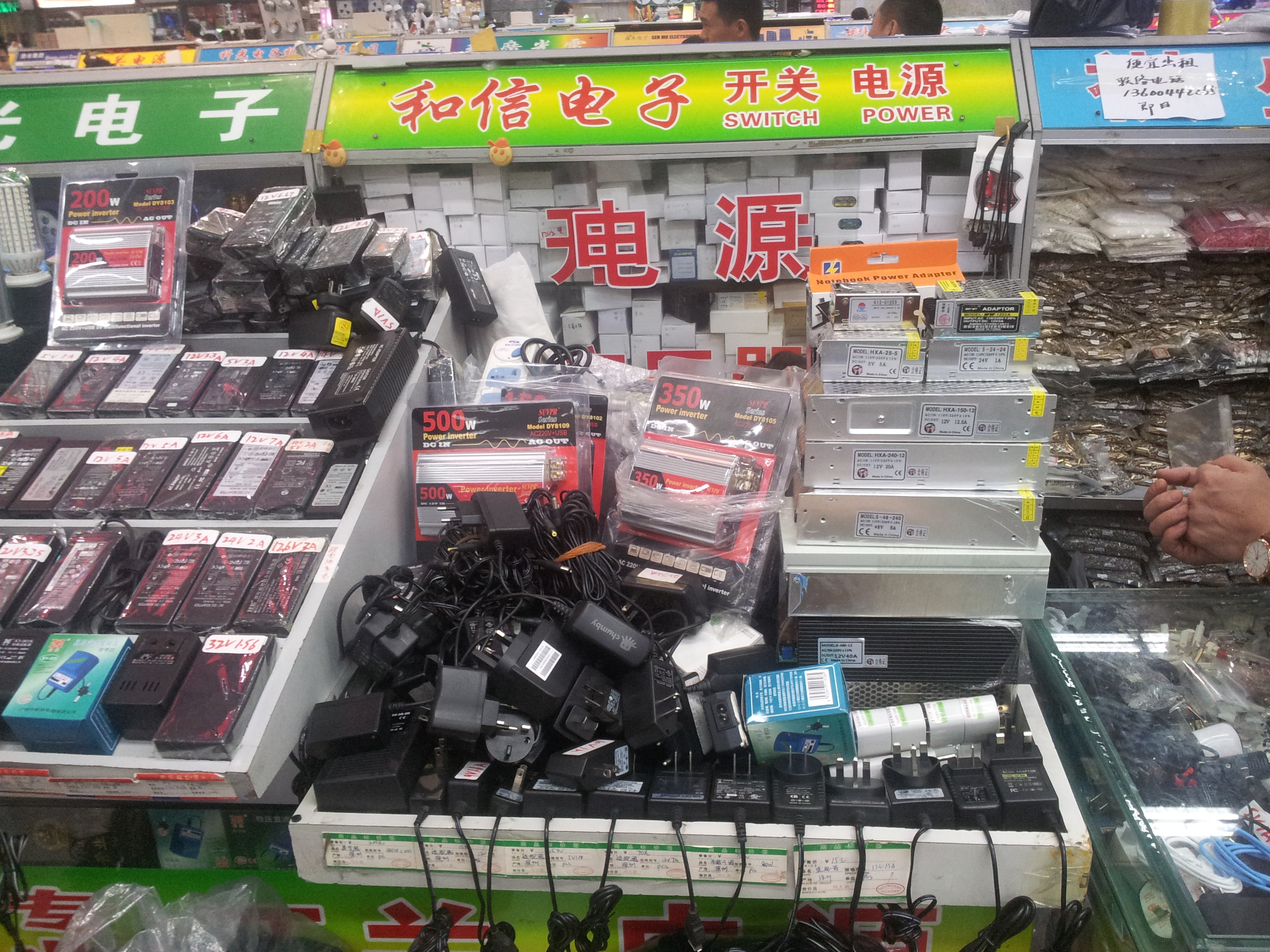

It’s the first time I’ve ever come across one of my former products in the Shenzhen markets. It’s kind of neat because I have intimate knowledge of how it might have ended up at this reseller’s stall. It also brought back old memories of agonizing over the logo color and placement — I think we tested over a half-dozen shades of gray before we settled on this one, and we had to fight with the printer to get the eyes just right and no smearing despite printing on a curved surface (accessories are in many ways harder than the product itself). Amusingly, this lady is selling the power supply for less than it cost us to originally buy it (you can just see the top of her head in the photo, she ducked behind the counter to find the power supplies we were buying, and I snapped the photo while she wasn’t looking).
Most of the excess inventory for this power supply ended up in the US office to handle exchanges & returns, so I’m pretty sure these are from a batch of power supplies that we had rejected. If I recall correctly, I had discovered an issue where one of the inductors in the power supply was missing the glob of glue required to hold it in place. Shipping the unit subjected the power supply to vibration, which caused the inductor to rub against a neighboring part. The rubbing could wear off the enamel on the inductor, which ultimately leads to the inductor shorting against the neighboring part. The power supply’s internal fuse correctly blows when this happens, so it wasn’t a safety issue; but the defectivity rate was around a few percent after shipping. I think a few thousand power supplies were sent back to the manufacturer over that issue. My guess is that after many years, the manufacturer finally found a sucker^H^H^H^H^H^H reseller who would peddle it in the markets.
Inspires confidence in the other ‘brand-name’ power supplies she was peddling, doesn’t it? On the other hand, I did buy a Lenovo-branded power supply that was perfect for my needs. ‘Brand new’ with plastic over the logos, it set me back only $4 a piece, and I did verify on the spot using a multimeter that the power supply did output the correct voltage. Probably good enough for development use, and at that price you just buy two in case one breaks.