Where Arduinos are Born: Touring a PCB Factory

August 14th, 2012

I recently had the pleasure and privilege of touring the factories that make Arduinos.

Arduinos are made in Scarmagno, Italy, a small town near the Olivetti factories on the outskirts of Torino. All of the circuit board fabrication, board stuffing and distribution is handled out of that small town. I was really excited to see the factories, and I’d like to share some photos of them with you.

The highlight of my tour was “System Electronica”, the PCB factory which makes the Arduino PCBs.

One charming aspect of System Electronica is the owner has the factory painted to match the colors of the Italian flag. In this wide view of the factory floor, you can see some of that in the red and white posts down the length of the facility.

Arduinos start as huge sheets of virgin copper-on-FR4.

The sheets above are 1.6mm thick (the most common thickness for a PCB, which corresponds to 1/16th of an inch), and probably a meter on one side by about a meter and a half.

The first step in processing is to drill the holes: hole drilling is done even before patterning. This is because once the holes are drilled, you can use the holes to align the masks used to pattern the traces later on in the process. Hole drilling is also a dirty and messy process, which can damage circuit patterns.

Above is the CNC drilling head used to drill the boards. The blank copper sheets are actually stacked three-high so a single pass of the drill can produce three substrates.

Above is the drill rack used by the CNC drilling machine. If you’ve ever had to muck around with creating NC-drill files, you’ll probably have seen the term “drill rack” used somewhere. This is what it looks like.

Above is the drill in action. It’s encoded in Ogg Theora; so, sorry if you’re using IE or Safari and you don’t have the codec installed. An HD version of the video is also available here. Flash is dead; long live HTML5! [note: I turned off video pre-loading to save bandwidth by just editing the attribute tags. That would have been a pain in Flash. Yet another benefit of HTML5!]

Every hole in the board is mechanically drilled, which is why via count is such an important parameter in calculating the cost of a PCB. This particular drill is a relatively small one. I’ve seen massive drill decks in China that slave four or six drill heads together in a truck-sized machine, processing dozens of panels at the same time; they drill so fast and hard that the ground shakes, even from several meters away, with every via drilled.

Above is a stack of finished, drilled boards that have been cleaned and deburred, ready for the next step in the process.

The next step is to apply a photoresist to the board and expose a pattern. At System Electronica, this is done using a light box and a high-contrast film. Other technologies I’ve seen include direct laser imaging, where the pattern is put on using a raster-scanning laser. Direct laser scanners are more common in quick-turn prototype houses, and film imaging is more common in mass production houses.

Above is a PCB blank being mounted into a light box for exposure. Note that most photos in this post can be clicked to reveal a much higher resolution version.

Above is what the board looks like before and after exposure.

The boards are then sent into a machine to be developed. In this case, the same machine is capable of developing both the photoresist and the soldermask.

Above is an image of a developed board. It’s one of my favorite photos out of the factory. Also, there is just something cool sounding about “Codice: Leonardo”.

After photo-processing and development, the boards go through a series of chemical baths that etch and plate the copper.

The movement of the boards through the chemical baths is fully automated; this is necessary because between certain steps oxygen can spoil a board in a matter of seconds, so the transfer between the baths needs to be fast. Also, the baths contain caustic and harmful chemicals to humans, so it’s much safer for a robot to do this work.

[HD verison] As you can see, the boards swish gently back and forth in the baths as they are processed. Each bath has a different solution in it.

Once the boards are processed in this series of solutions, a dull, white plating (which I’m guessing is nickel) has developed on all the non-resist covered surfaces of the board, including the previously unplated vias and pads.

At this point the resist and unplated copper is stripped off, leaving just the raw FR-4 and the plated copper.

A final step of processing results in a bright copper finish. Note that the photo above isn’t of an Arduino board, as their boards weren’t going through the machine at the time when I was taking photos of it.

The boards are now ready to have soldermask and silkscreen applied. These are applied using a very similar process to the trace patterns, using a photomask and developer/stripper machine.

Above is photo showing a board with both soldermask and “silkscreen” developed. The silkscreen in this case is actually a second layer of soldermask. A very specific formulation of dry-film white soldermask was procured for team Arduino to create a sharp and good-looking layer that can resolve the intricate artwork found on Arduino boards. Other techniques I’ve seen for producing silkscreen layers include high resolution inkjet printing, which is better suited for quick-turn board houses, and of course the namesake squeegee-and-paint silkscreen process.

Once the boards have finished chemical processing, they receive a protective plating of solder through a hot-air solder leveling machine, and then move on to testing.

[HD version] Every board is 100% tested. This means that every trace has its continuity and resistance measured using a pair of flying probes. That’s a lot of probing, and the video above gives you an idea of how fast the probing is done. An alternative to flying head testing is to use clamshell testers, where a set of pogo pins are put into a fixture that can test the entire board with a single mechanical operation. However, clamshell fixtures are very labor-intensive to assemble and maintain, and require physical rewiring every time the gerbers are updated. So, in many cases flying probe testing can be cost-favorable and more flexible when compared to fixtured testing.

Above is a stack of near-finished PCB panels, ready for a final step of routing.

Before the boards can be shipped, the individual PCBs panels need to be routed so they can fit inside SMT machines. The boards are once again stacked up and batch-processed through a machine that uses a router bit to cut and release the board panels.

Finally, the boards are ready to ship on to the SMT facility. As you can see, the boards are panelized in a 2×6 format to make SMT processing more efficient.

Here’s a veritable stack of about 25,000 bare Arduino PCBs ready to leave the PCB factory, moving on to be stuffed, shipped and sold to Makers the world around!

Many thanks to the Officine Arduino team and Davide Gomba in particular for taking time out of their busy schedules, showing me around, and patiently waiting as I expressed my inner shutterbug and general love for all things hardware…

Name that Ware July 2012

July 16th, 2012

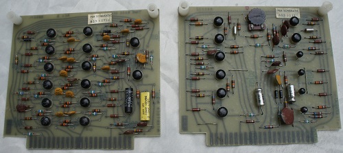
The ware for July 2012 is shown below.

I was cleaning up the basement of the home where I grew up, and came across some old childhood memories. I figured some of them might make fun wares to guess. Both items shown are from the same machine.

Winner, Name that Ware June 2012

July 16th, 2012

The ware for June 2012 was the control board from a GE PSC23SGPA-SS refrigerator. The part number of the control board is EBX1005G01 / REV N, made by Delphi electronics.

The control board was extracted from a fridge that failed. On the backside, one can see at least part of the cause of failure.

This is the solder joint from one of the larger relays. The joint had failed catastrophically, splattering bits of solder around the board. Replacing the board restored the fridge’s functionality.

All the comments about the complexity of the fridge controller board reminds me of Marvin from the Hitchiker’s Guide to the Galaxy: here I am, brain the size of a planet, and they ask me to…mind the fridge. Maybe the controller board committed suicide out of boredom.

The winner of last June’s competition is nrp. The link provided is to this exact model of board, but with a different revision. Congrats, email me for your prize!

Name that Ware June 2012

June 23rd, 2012

The Ware for June 2012 is shown below.

Thanks to Yi-Fang for sharing this with me!

Winner, Name that Ware May 2012

June 23rd, 2012

The Ware for May 2012 was a BGA re-balling tool. I picked this one up in Hua Qian Bei for about 80 RMB (~US$12), including stencils, balls, and other accessories. The lady who sold it to me was even nice enough to give me a little training on reballing.

I first encountered this tool being used in a factory to re-ball GDDR5 memory. The factory produced a line of graphics cards, and the memory was being stripped from graphics cards where the GPU failed test and were deemed un-salvageable. Before seeing this, I was under the impression that reballing was an involved process, but with this jig the operator could strip and reball a chip in under a few minutes, which translates to a labor cost of a couple dozen cents. This also explains how so many cheap SoCs end up for sale in the gray market — most of them are extracted from used phones, reballed, and re-packaged into tape and reel and sold as new. Given that a legitimate, brand new reel of these chips has a fair market value equivalent to an entry-level automobile, it’s now easy for me to understand the profit motive behind such efforts.

zyp got the answer very quickly, and is the prize winner, but I’m also giving a second honorary prize to sanjay, for the most entertaining explanation of what BGA reballing is:

BGA is the Ball Gilders Association.

As the name implies, it is a trade association of Ball Gilders. If you have never heard of them before, it is because they cater to a very exclusive clientele comprising some of the most discerning billionaires on this planet (millionaires need not apply).

Gilded Balls are the ultimate bling for a young man in his prime, and guaranteed to make an impact on the exclusive young ladies in your life.

However, the downside is that sometimes a gentleman will awaken after a night of revelry, and find his balls have been stolen.

This is where the reballer comes in. We have an exclusive range of prosthetic balls made of Gutta Percha, which we will install (at no additional cost) for any of our esteemed clients who have been unfortunate enough to have their ball stolen by one of the despicable 99% we happen to (unfortunately) have to share this planet with.

That’s just hilarious. Congrats, email me for your prize.